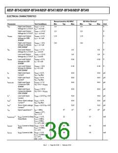
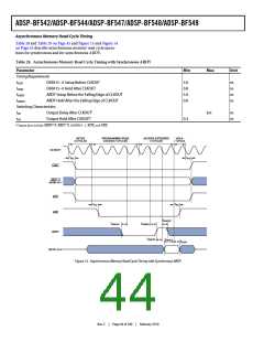
ADSP-BF542/ADSP-BF544/ADSP-BF547/ADSP-BF548/ADSP-BF549
the Total Current Pin Groups table. Note that the VOL and VOH
ABSOLUTE MAXIMUM RATINGS
specifications have separate per-pin maximum current require-
ments, see the Electrical Characteristics table.
Stresses greater than those listed in Table 21 may cause perma-
nent damage to the device. These are stress ratings only.
Functional operation of the device at these or any other condi-
tions greater than those indicated in the operational sections of
this specification is not implied. Exposure to absolute maximum
rating conditions for extended periods may affect device reli-
ability. Table 22 details the maximum duty cycle for input
transient voltage.
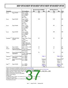
Table 23. Total Current Pin Groups
Group Pins in Group
1
2
3
PA0, PA1, PA2, PA3, PA4, PA5, PA6, PA7, PA8, PA9, PA10,
PA11
PA12, PA13, PA14, PA15, PB8, PB9, PB10, PB11, PB12,
PB13, PB14
Table 21. Absolute Maximum Ratings
PB0, PB1, PB2, PB3, PB4, PB5, PB6, PB7, BMODE0,
BMODE1, BMODE2, BMODE3
Internal (Core) Supply Voltage (VDDINT) –0.3 V to +1.43 V
External (I/O) Supply Voltage (VDDEXT) –0.3 V to +3.8 V
4
TCK, TDI, TDO, TMS, TRST, PD14, EMU
PD8, PD9, PD10, PD11, PD12, PD13, PD15
PD0, PD1, PD2, PD3, PD4, PD5, PD6, PD7
PE11, PE12, PE13, PF12, PF13, PF14, PF15, PG3, PG4
PF4, PF5, PF6, PF7, PF8, PF9, PF10, PF11
PF0, PF1, PF2, PF3, PG0, PG1, PG2
PC0, PC1, PC2, PC3, PC4, PC5, PC6, PC7
PH5, PH6, PH7
Input Voltage1, 2, 3
–0.5 V to +3.6 V
–0.5 V to VDDEXT +0.5 V
40 mA (max)
5
Output Voltage Swing
IOH/IOL Current per Single Pin4
6
7
I
OH/IOL Current per Pin Group4
80 mA (max)
8
Storage Temperature Range
–65ºC to +150ºC
9
Junction Temperature Underbias
+125ºC
10
11
12
13
14
15
16
17
18
19
20
21
22
23
24
25
1 AppliestoallbidirectionalandinputonlypinsexceptPB1-0, PE15-14, PG15–11,
and PH7-6, where the absolute maximum input voltage range is –0.5 V to
+5.5 V.
A1, A2, A3
2 Pins USB_DP, USB_DM, and USB_VBUS are 5 V-tolerant when VDDUSB is
powered according to the operating conditions table. If VDDUSB supply
voltage does not meet the specification in the operating conditions table, these
pins could suffer long-term damage when driven to +5 V. If this condition is
seen in the application, it can be corrected with additional circuitry to use the
external host to power only the VDDUSB pins. Contact factory for application
detail and reliability information.
PH8, PH9, PH10, PH11, PH12, PH13
PI0, PI1, PI2, PI3, PI4, PI5, PI6, PI7
PI8, PI9, PI10, PI11, PI12, PI13, PI14, PI15
AMS0, AMS1, AMS2, AMS3, AOE, CLKBUF, NMI
CLKIN, XTAL, RESET, RTXI, RTXO, ARE, AWE
D0, D1, D2, D3, D4, D5, D6, D7
3 Applies only when VDDEXT is within specifications. When VDDEXT is outside speci-
fications, the range is VDDEXT 0.2 V.
4 For more information, see description preceding Table 23.
D8, D9, D10, D11, D12
D13, D14, D15, ABE0, ABE1
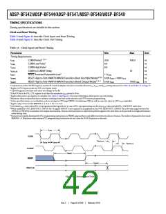
Table 22. Maximum Duty Cycle for Input1 Transient Voltage
EXT_WAKE, CLKOUT, PJ11, PJ12, PJ13
PJ0, PJ1, PJ2, PJ3, PJ4, PJ5, PJ6, PJ7, ATAPI_PDIAG
PJ8, PJ9, PJ10, PE7, PG12, PG13
VIN Max (V)2
3.63
VIN Min (V)
–0.33
Maximum Duty Cycle
100%
48%
30%
20%
10%
8%
PE0, PE1, PE2, PE4, PE5, PE6, PE8, PE9, PE10, PH3, PH4
3.80
–0.50
PH0, PH2, PE14, PE15, PG5, PG6, PG7, PG8, PG9, PG10,
PG11
3.90
–0.60
4.00
–0.70
26
PC8, PC9, PC10, PC11, PC12, PC13, PE3, PG14, PG15, PH1
4.10
–0.80
4.20
–0.90
4.30
–1.00
5%
1 Does not apply to CLKIN. Absolute maximum for pins PB1-0, PE15-14, PG15-
11, and PH7-6 is +5.5V.
2 Only one of the listed options can apply to a particular design.
The Absolute Maximum Ratings table specifies the maximum
total source/sink (IOH/IOL) current for a group of pins. Perma-
nent damage can occur if this value is exceeded. To understand
this specification, if pins PA4, PA3, PA2, PA1 and PA0 from
group 1 in the Total Current Pin Groups table were sourcing or
sinking 2 mA each, the total current for those pins would be
10 mA. This would allow up to 70 mA total that could be
sourced or sunk by the remaining pins in the group without
damaging the device. For a list of all groups and their pins, see
Rev. C
|
Page 40 of 100
|
February 2010

 ADI [ ADI ]