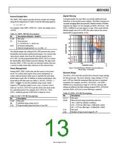
ADIS16362
THEORY OF OPERATION
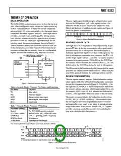
The user registers provide addressing for all input/output opera-
tions on the SPI interface. Each 16-bit register has two 7-bit
addresses: one for its upper byte and one for its lower byte.
Table 8 lists the lower byte address for each register, and Figure 10
shows the generic bit assignments.
BASIC OPERATION
The ADIS16362 is an autonomous sensor system that starts up
after it has a valid power supply voltage and begins producing
inertial measurement data at the factory default sample rate
setting of 819.2 SPS. After each sample cycle, the sensor data is
loaded into the output registers, and DIO1 pulses high, which
provides a new data ready control signal for driving system-
level interrupt service routines. In a typical system, a master
processor accesses the output data registers through the SPI
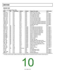
interface, using the connection diagram shown in Figure 9.
Table 6 provides a generic functional description for each pin
on the master processor. Table 7 describes the typical master
processor settings that are normally found in a configuration
register and used for communicating with the ADIS16362.
I/O LINES ARE COMPATIBLE WITH
15 14 13 12 11 10
9
8
7
6
5
4
3
2
1
0
UPPER BYTE
LOWER BYTE
Figure 10. Generic Register Bit Assignments
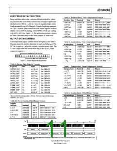
READING SENSOR DATA
Although the ADIS16362 produces data independently, it oper-
ates as a SPI slave device that communicates with system (master)
processors using the 16-bit segments displayed in Figure 11.
Individual register reads require two of these 16-bit sequences. The
R
first 16-bit sequence provides the read command bit ( /W = 0)
5V
3.3V OR 5V LOGIC LEVELS
VDD
and the target register address (A6 to A0). The second sequence
transmits the register contents (D15 to D0) on the DOUT line.
For example, if DIN = 0x0A00, the contents of XACCL_OUT are
shifted out on the DOUT line during the next 16-bit sequence.
10
11
12
SYSTEM
PROCESSOR
SPI MASTER
ADIS16362
SPI SLAVE
6
3
5
4
7
SS
CS
SCLK
MOSI
SCLK
DIN
The SPI operates in full-duplex mode, which means that the master
processor can read the output data from DOUT while using the
same SCLK pulses to transmit the next target address on DIN.
MISO
IRQ
DOUT
DIO1
13
DEVICE CONFIGURATION
14
15
The user register memory map (see Table 8) identifies configu-
ration registers with either a W or R/W. Configuration commands
also use the bit sequence shown in Figure 11. If the MSB = 1, the
last eight bits (DC7 to DC0) in the DIN sequence are loaded into
the memory address associated with the address bits (A6 to A0).
For example, if DIN = 0xA11F, 0x1F is loaded into Address 0x21
(XACCL_OFF, upper byte) at the conclusion of the data frame.
Figure 9. Electrical Connection Diagram
Table 6. Generic Master Processor Pin Names and Functions
Pin Name
Function
SS
Slave select
IRQ
Interrupt request
Master output, slave input
Master input, slave output
Serial clock
The master processor initiates the backup function by setting
GLOB_CMD[3] = 1 (DIN = 0xBE04). This command copies
the user registers into their assigned flash memory locations
and requires the power supply to stay within its normal operating
range for the entire 50 ms process. The FLASH_CNT register
provides a running count of these events for monitoring the
long-term reliability of the flash memory.
MOSI
MISO
SCLK
Table 7. Generic Master Processor SPI Settings
Processor Setting
Description
Master
The ADIS±ꢃ3ꢃ2 operates as a slave
Normal mode, SMPL_PRD[ꢁ:0] ≤ 0x09
CPOL = ± (polarity), CHPA = ± (phase)
Bit sequence
SCLK Rate ≤ 2 MHz±
SPI Mode 3
MSB First Mode
±ꢃ-Bit Mode
Shift register/data length
± For burst read, SCLK rate ≤ ± MHz. For low power mode, SCLK rate ≤ 300 kHz.
CS
SCLK
DIN
DOUT
NOTES
R/W A6
A5
R/W A6
D14
A5
A4
A3
A2
A1
D9
A0 DC7 DC6 DC5 DC4 DC3 DC2 DC1 DC0
D8 D7 D6 D5 D4 D3 D2 D1 D0
D15 D14 D13
D15
D13 D12 D11 D10
1. DOUT BITS ARE BASED ON THE PREVIOUS 16-BIT SEQUENCE (R = 0).
Figure 11. SPI Communication Bit Sequence
Rev. 0 | Page 9 of 20

 ADI [ ADI ]