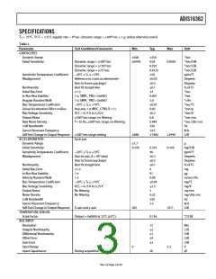
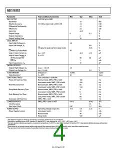
ADIS16362
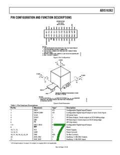
PIN CONFIGURATION AND FUNCTION DESCRIPTIONS
ADIS16362
TOP VIEW
(Not to Scale)
1
2
3
4
5
6
7
8
9
11 13 15 17 19 21 23
10 12 14 16 18 20 22 24
NOTES
1. THIS REPRESENTATION DISPLAYS THE TOP VIEW PINOUT
FOR THE MATING SOCKET CONNECTOR.
2. THE ACTUAL CONNECTOR PINS ARE NOT VISIBLE FROM
THE TOP VIEW.
3. MATING CONNECTOR: SAMTEC CLM-112-02 OR EQUIVALENT.
4. DNC = DO NOT CONNECT.
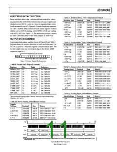
Figure 5. Pin Configuration
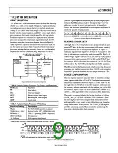
Z-AXIS
aZ
gZ
Y-AXIS
aY
X-AXIS
aX
gY
gX
PIN 23
ORIGIN ALIGNMENT REFERENCE POINT
SEE MSC_CTRL[6].
PIN 1
NOTES
1. ACCELERATION (aX
,
aY, aZ) AND ROTATIONAL (gX, gY, gZ) ARROWS
INDICATE THE DIRECTION OF MOTION THAT PRODUCES
A POSITIVE OUTPUT.
Figure 6. Axial Orientation
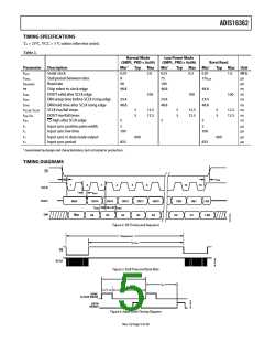
Table 5. Pin Function Descriptions
Pin No.
Mnemonic
Type1
Description
Configurable Digital Input/Output.
±
DIO3
I/O
2
3
DIO4/CLKIN
SCLK
I/O
I
Configurable Digital Input/Output or Sync Clock Input.
SPI Serial Clock.
4
ꢀ
ꢃ
DOUT
DIN
CS
O
I
I
SPI Data Output. Clocks output on SCLK falling edge.
SPI Data Input. Clocks input on SCLK rising edge.
SPI Chip Select.
ꢁ, 9
8
DIO±, DIO2
RST
I/O
I
Configurable Digital Input/Output.
Reset.
±0, ±±, ±2
VCC
S
Power Supply.
±3, ±4, ±ꢀ
GND
S
Power Ground.
±ꢃ, ±ꢁ, ±8, ±9, 22, 23, 24
DNC
N/A
Do Not Connect.
20
2±
AUX_DAC
AUX_ADC
O
I
Auxiliary, ±2-Bit DAC Output.
Auxiliary, ±2-Bit ADC Input.
± I/O is input/output, I is input, O is output, S is supply, N/A is not applicable.
Rev. 0 | Page ꢁ of 20

 ADI [ ADI ]