ADIS16362
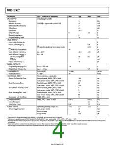
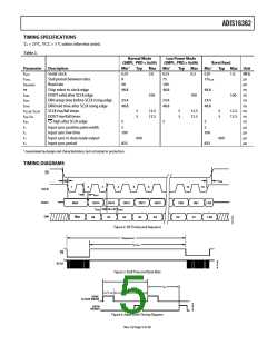
TIMING SPECIFICATIONS
TA = 25°C, VCC = 5 V, unless otherwise noted.
Table 2.
Normal Mode
(SMPL_PRD ≤ 0x09)
Low Power Mode
(SMPL_PRD ≥ 0x0A)
Burst Read
Typ Max Unit
Parameter
Description
Min1
0.0±
9
Typ
Max
Min±
0.0±
ꢁꢀ
Typ
Max
Min±
0.0±
fSCLK
tSTALL
tREADRATE
tCS
tDAV
tDSU
tDHD
tSCLKR, tSCLKF
tDR, tDF
tSFS
Serial clock
Stall period between data
Read rate
Chip select to clock edge
DOUT valid after SCLK edge
DIN setup time before SCLK rising edge
DIN hold time after SCLK rising edge
SCLK rise/fall times
2.0
0.3
±.0
MHz
μs
μs
ns
ns
ns
ns
ns
ns
ns
μs
μs
μs
μs
±/fSCLK
40
±00
48.8
48.8
48.8
±00
±00
±00
24.4
48.8
24.4
48.8
24.4
48.8
ꢀ
ꢀ
±2.ꢀ
±2.ꢀ
ꢀ
ꢀ
±2.ꢀ
±2.ꢀ
ꢀ
ꢀ
±2.ꢀ
±2.ꢀ
DOUT rise/fall times
CS high after SCLK edge
Input sync positive pulse width
Input sync low time
ꢀ
ꢀ
ꢀ
t±
tx
ꢀ
±00
ꢀ
±00
t2
t3
Input sync to data ready output
Input sync period
ꢃ00
ꢃ00
833
833
± Guaranteed by design and characterization, but not tested in production.
TIMING DIAGRAMS
CS
tCS
tSFS
1
2
3
4
5
6
15
16
SCLK
DOUT
tDAV
MSB
DB14
tDSU
DB13
A5
DB12
DB11
DB10
DB2
DB1
D1
LSB
LSB
tDHD
DIN
R/W
A6
A4
A3
A2
D2
Figure 2. SPI Timing and Sequence
tREADRATE
tSTALL
CS
SCLK
Figure 3. Stall Time and Data Rate
t3
t2
t1
tX
SYNC
CLOCK (DIO4)
DATA
READY
Figure 4. Input Clock Timing Diagram
Rev. 0 | Page ꢀ of 20

 ADI [ ADI ]