ADIS16362
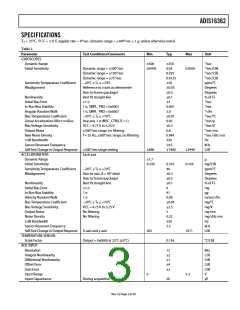
Parameter
Test Conditions/Comments
Min
Typ
Max
Unit
DAC OUTPUT
ꢀ kΩ/±00 pF to GND
Resolution
±2
±4
±±
±ꢀ
Bits
LSB
LSB
mV
%
Relative Accuracy
Differential Nonlinearity
Offset Error
±0± LSB ≤ input code ≤ 409ꢀ LSB
Gain Error
±0.ꢀ
Output Range
0
3.3
V
Output Impedance
Output Settling Time
LOGIC INPUTS±
Input High Voltage, VIH
Input Low Voltage, VIL
2
±0
Ω
μs
2.0
20
V
V
V
0.8
0.ꢀꢀ
CS signal to wake up from sleep mode
CS Wake-Up Pulse Width
Logic ± Input Current, IIH
Logic 0 Input Current, IIL
All Pins Except RST
μs
μA
VIH = 3.3 V
VIL = 0 V
±0.2
±±0
ꢃ0
40
±
ꢄA
mA
pF
RST Pin
Input Capacitance, CIN
DIGITAL OUTPUTS±
Output High Voltage, VOH
Output Low Voltage, VOL
FLASH MEMORY
±0
ISOURCE = ±.ꢃ mA
ISINK = ±.ꢃ mA
Endurance2
TJ = 8ꢀ°C
2.4
V
V
0.4
±0,000
20
Cycles
Years
Data Retention3
FUNCTIONAL TIMES4
Power-On Start-Up Time
Time until data is available
Normal mode, SMPL_PRD ≤ 0x09
Low power mode, SMPL_PRD ≥ 0x0A
Normal mode, SMPL_PRD ≤ 0x09
Low power mode, SMPL_PRD ≥ 0x0A
Normal mode, SMPL_PRD ≤ 0x09
Low power mode, SMPL_PRD ≥ 0x0A
Normal mode, SMPL_PRD ≤ 0x09
Low power mode, SMPL_PRD ≥ 0x0A
SMPL_PRD = 0x0±
±80
2ꢀ0
ꢃ0
±30
4
ms
ms
ms
ms
ms
ms
ms
ms
ms
SPS
%
Reset Recovery Time
Sleep Mode Recovery Time
Flash Memory Test Time
9
±ꢁ
90
±2
Automatic Self-Test Time
CONVERSION RATE
Clock Accuracy
SMPL_PRD = 0x0± to 0xFF
0.4±3
8±9.2
±3
Sync Input Clock
0.8ꢀ
4.ꢁꢀ
±.2
kHz
V
mA
mA
μA
POWER SUPPLY
Power Supply Current
Operating voltage range, VCC
Low power mode
Normal mode
ꢀ.0
24
49
ꢀ.2ꢀ
Sleep mode
ꢀ00
± The digital I/O signals are driven by an internal 3.3 V supply, and the inputs are ꢀ V tolerant.
2 Endurance is qualified as per JEDEC Standard 22, Method A±±ꢁ, and measured at −40°C, +2ꢀ°C, +8ꢀ°C, and +±2ꢀ°C.
3 The data retention lifetime equivalent is at a junction temperature (TJ) of 8ꢀ°C as per JEDEC Standard 22, Method A±±ꢁ. Data retention lifetime decreases with junction
temperature.
4 These times do not include thermal settling and internal filter response times (330 Hz bandwidth), which may affect overall accuracy.
ꢀ The sync input clock functions below the specified minimum value, at reduced performance levels.
Rev. 0 | Page 4 of 20

 ADI [ ADI ]