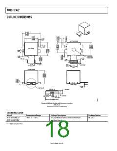
ADIS16362
APPLICATIONS INFORMATION
INSTALLATION/HANDLING
For ADIS16362 installation, use the following two-step process:
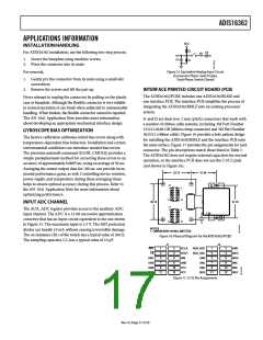
VCC
D
C2
R1
1. Secure the baseplate using machine screws.
2. Press the connector into its mate.
C1
D
Figure 15. Equivalent Analog Input Circuit
(Conversion Phase: Switch Open,
Track Phase: Switch Closed)
For removal,
1. Gently pry the connector from its mate using a small slot
screwdriver.
2. Remove the screws and lift the part up.
INTERFACE PRINTED CIRCUIT BOARD (PCB)
The ADIS16362/PCBZ includes one ADIS16362BLMZ and
one interface PCB. The interface PCB simplifies the process of
integrating the ADIS16362BMLZ into an existing processor
system.
Never attempt to unplug the connector by pulling on the plastic
case or baseplate. Although the flexible connector is very reliable
in normal operation, it can break when subjected to unreasonable
handling. When broken, the flexible connector cannot be repaired.
The AN-1041 Application Note provides more information
about developing an appropriate mechanical interface design.
J1 and J2 are dual-row, 2 mm (pitch) connectors that work with
a number of ribbon cable systems, including 3M Part Number
152212-0100-GB (ribbon crimp connector) and 3M Part Number
3625/12 (ribbon cable). Figure 16 provides a hole pattern design
for installing the ADIS16362BMLZ and the interface PCB onto
the same surface. Figure 17 provides the pin assignments for each
connector. The pin descriptions match those listed in Table 5.
The ADIS16362 does not require external capacitors for normal
operation, so the interface PCB does not use the C1/C2 pads
(not shown in Figure 16).
GYROSCOPE BIAS OPTIMIZATION
The factory calibration addresses initial bias errors along with
temperature-dependent bias behaviors. Installation and certain
environmental conditions can introduce modest bias errors.
The precision autonull command (GLOB_CMD[4]) provides a
simple predeployment method for correcting these errors to an
accuracy of approximately 0.008°/sec, using an average of 30 sec.
Averaging the sensor output data for 100 sec can provide incre-
mental performance gains, as well. Controlling device rotation,
power supply, and temperature during these averaging times
helps to ensure optimal accuracy during this process. Refer to
the AN-1041 Application Note for more information about
optimizing performance.
23.75
21.24
J2
1
2
11
12
2
30.10
27.70
INPUT ADC CHANNEL
J1
1
The AUX_ADC register provides access to the auxiliary ADC
input channel. The ADC is a 12-bit successive approximation
converter that has an input circuit equivalent to the one shown
in Figure 15. The maximum input is 3.3 V. The ESD protection
diodes can handle 10 mA without causing irreversible damage.
The on resistance (R1) of the switch has a typical value of 100 Ω.
The sampling capacitor, C2, has a typical value of 16 pF.
1.20
11
12
NOTES
1. DIMENSIONS IN MILLIMETERS.
Figure 16. Physical Diagram for the ADIS16362/PCBZ
J1
J2
RST
CS
1
3
2
4
SCLK
DOUT
DIN
AUX_ADC
AUX_DAC
GND
1
3
2
4
GND
DIO3
DIO4
DNC
DNC
DIO1
DNC
GND
GND
VCC
5
6
5
6
7
8
GND
VCC
VCC
DNC
7
8
9
10
12
DNC
9
10
12
11
DIO2
11
Figure 17. J1/J2 Pin Assignments
Rev. 0 | Page 17 of 20

 ADI [ ADI ]