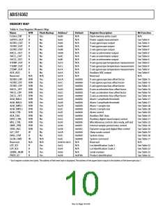
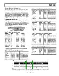
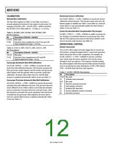
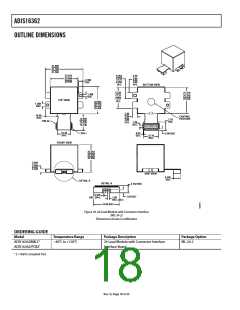
ADIS16362
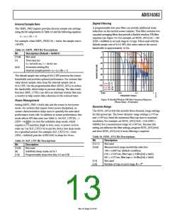
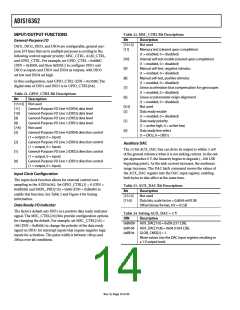
Table 22. MSC_CTRL Bit Descriptions
INPUT/OUTPUT FUNCTIONS
Bit
Description
General-Purpose I/O
[±ꢀ:±2]
[±±]
Not used
DIO1, DIO2, DIO3, and DIO4 are configurable, general-pur-
pose I/O lines that serve multiple purposes according to the
following control register priority: MSC_CTRL, ALM_CTRL,
and GPIO_CTRL. For example, set GPIO_CTRL = 0x080C
(DIN = 0xB308, and then 0xB20C) to configure DIO1 and
DIO2 as inputs and DIO3 and DIO4 as outputs, with DIO3
set low and DIO4 set high.
Memory test (cleared upon completion)
(± = enabled, 0 = disabled)
Internal self-test enable (cleared upon completion)
(± = enabled, 0 = disabled)
Manual self-test, negative stimulus
(± = enabled, 0 = disabled)
Manual self-test, positive stimulus
(± = enabled, 0 = disabled)
Linear acceleration bias compensation for gyroscopes
(± = enabled, 0 = disabled)
Linear accelerometer origin alignment
(± = enabled, 0 = disabled)
Not used
Data ready enable
(± = enabled, 0 = disabled)
Data ready polarity
(± = active high, 0 = active low)
Data ready line select
(± = DIO2, 0 = DIO±)
[±0]
[9]
[8]
[ꢁ]
[ꢃ]
In this configuration, read GPIO_CTRL (DIN = 0x3200).The
digital state of DIO1 and DIO2 is in GPIO_CTRL[9:8].
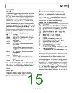
Table 21. GPIO_CTRL Bit Descriptions
Bit
Description
[±ꢀ:±2] Not used
[ꢀ:3]
[2]
[±±]
[±0]
[9]
[8]
[ꢁ:4]
[3]
General-Purpose I/O Line 4 (DIO4) data level
General-Purpose I/O Line 3 (DIO3) data level
General-Purpose I/O Line 2 (DIO2) data level
General-Purpose I/O Line ± (DIO±) data level
Not used
General-Purpose I/O Line 4 (DIO4) direction control
(± = output, 0 = input)
[±]
[0]
[2]
[±]
[0]
General-Purpose I/O Line 3 (DIO3) direction control
(± = output, 0 = input)
General-Purpose I/O Line 2 (DIO2) direction control
(± = output, 0 = input)
General-Purpose I/O Line ± (DIO±) direction control
(± = output, 0 = input)
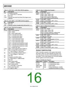
Auxiliary DAC
The 12-bit AUX_DAC line can drive its output to within 5 mV
of the ground reference when it is not sinking current. As the out-
put approaches 0 V, the linearity begins to degrade (~100 LSB
beginning point). As the sink current increases, the nonlinear
range increases. The DAC latch command moves the values of
the AUX_DAC register into the DAC input register, enabling
both bytes to take effect at the same time.
Input Clock Configuration
The input clock function allows for external control over-
sampling in the ADIS16362. Set GPIO_CTRL[3] = 0 (DIN =
0x0B200) and SMPL_PRD[7:0] = 0x00 (DIN = 0xB600) to
enable this function. See Table 2 and Figure 4 for timing
information.
Table 23. AUX_DAC Bit Descriptions
Bit
Description
[±ꢀ:±2]
[±±:0]
Not used
Data bits, scale factor = 0.80ꢀ9 mV/LSB
Offset binary format, 0 V = 0 LSB
Data Ready I/O Indicator
The factory default sets DIO1 as a positive data ready indicator
signal. The MSC_CTRL[2:0] bits provide configuration options
for changing the default. For example, set MSC_CTRL[2:0] =
100 (DIN = 0xB404) to change the polarity of the data ready
signal on DIO1 for interrupt inputs that require negative logic
inputs for activation. The pulse width is between 100 μs and
200 μs over all conditions.
Table 24. Setting AUX_DAC = 1 V
DIN Description
0xB0D9 AUX_DAC[ꢁ:0] = 0xD9 (2±ꢁ LSB).
0xB±04
0xBE04
AUX_DAC[±ꢀ:8] = 0x04 (±024 LSB).
GLOB_CMD[2] = ±.
Move values into the DAC input register, resulting in
a ± V output level.
Rev. 0 | Page ±4 of 20

 ADI [ ADI ]