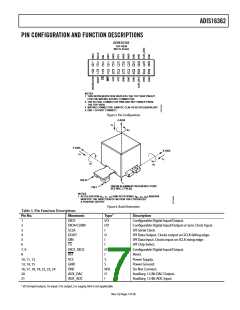
ADIS16362
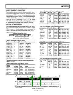
BURST READ DATA COLLECTION
Table 11. Rotation Rate, Twos Complement Format
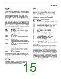
Burst read data collection is a process-efficient method for collect-
ing data from the ADIS16362. In burst read, all output registers are
clocked out on DOUT, 16 bits at a time, in sequential data cycles
(each separated by one SCLK period). To start a burst read sequence,
set DIN = 0x3E00. The contents of each output register are then
shifted out on DOUT, starting with SUPPLY_OUT and ending
with AUX_ADC (see Figure 13). The addressing sequence shown
in Table 8 determines the order of the outputs in burst read.
Rotation Rate
+300°/sec
+0.±°/sec
+0.0ꢀ°/sec
0°/sec
−0.0ꢀ°/sec
−0.±°/sec
−300°/sec
Decimal
+ꢃ000 LSB
+2 LSB
+± LSB
0 LSB
−± LSB
−2 LSB
−ꢃ000 LSB
Hex
Binary
0x±ꢁꢁ0 XX0± 0±±± 0±±± 0000
0x0002 XX00 0000 0000 00±0
0x000± XX00 0000 0000 000±
0x0000 XX00 0000 0000 0000
0x3FFF
0x3FFE
XX±± ±±±± ±±±± ±±±±
XX±± ±±±± ±±±± ±±±0
0x2890 XX±0 ±000 ±00± 0000
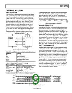
OUTPUT DATA REGISTERS
Each output data register uses the format in Figure 12 and Table 9.
Figure 6 shows the positive direction for each inertial sensor. The
ND bit is equal to 1 when the register contains unread data. The
EA bit is high when any error/alarm flag in the DIAG_STAT
register is equal to 1.
Table 12. Acceleration, Twos Complement Format
Acceleration
Decimal
+ꢀ±0ꢀ LSB
+2 LSB
+± LSB
0 LSB
Hex
Binary
+±.ꢁ g
0x±3F±
XX0± 00±± ±±±± 000±
+0.ꢃꢃꢁ mg
+0.333 mg
0 g
0x0002 XX00 0000 0000 00±0
0x000± XX00 0000 0000 000±
0x0000 XX00 0000 0000 0000
MSB FOR 14-BIT OUTPUT
ND EA
−0.333 mg
−0.ꢃꢃꢁ mg
−±.ꢁ g
−± LSB
−2 LSB
−ꢀ±0ꢀ LSB
0x3FFF
0x3FFE
XX±± ±±±± ±±±± ±±±±
XX±± ±±±± ±±±± ±±±0
MSB FOR 12-BIT OUTPUT
Figure 12. Output Register Bit Assignments
0x2C0F XX±0 ±±00 0000 ±±±±
Table 9. Output Data Register Formats
Table 13. Temperature, Twos Complement Format
Register
Bits
Scale
Reference
Temperature
Decimal
+ꢀ88 LSB
+44± LSB
+2 LSB
+± LSB
0 LSB
−± LSB
−2 LSB
−4ꢁ8 LSB
Hex
Binary
SUPPLY_OUT
±2
2.4±8 mV
0.0ꢀ°/sec
0.0ꢀ°/sec
0.0ꢀ°/sec
0.333 mg
0.333 mg
0.333 mg
0.±3ꢃ°C
See Table ±0
See Table ±±
See Table ±±
See Table ±±
See Table ±2
See Table ±2
See Table ±2
See Table ±3
See Table ±3
See Table ±3
See Table ±4
XGYRO_OUT± ±4
YGYRO_OUT± ±4
ZGYRO_OUT± ±4
+±0ꢀ°C
+8ꢀ°C
0x24C
0x±B9
0x002
0x00±
0x000
0xFFF
0xFFE
0xE22
XXXX 00±0 0±00 ±±00
XXXX 000± ±0±± ±00±
XXXX 0000 0000 00±0
XXXX 0000 0000 000±
XXXX 0000 0000 0000
XXXX ±±±± ±±±± ±±±±
XXXX ±±±± ±±±± ±±±0
XXXX ±±±0 00±0 00±0
+2ꢀ.2ꢁ2°C
+2ꢀ.±3ꢃ°C
+2ꢀ°C
+24.8ꢃ4°C
+24.ꢁ28°C
−40°C
XACCL_OUT
YACCL_OUT
ZACCL_OUT
XTEMP_OUT2 ±2
YTEMP_OUT2 ±2
ZTEMP_OUT2 ±2
±4
±4
±4
0.±3ꢃ°C
0.±3ꢃ°C
80ꢀ.8 μV
AUX_ADC
±2
Table 14. Analog Input, Offset Binary Format
± Assumes that the scaling is set to ±300°/sec. This factor scales with the range.
2 0x0000 = 2ꢀ°C (±ꢀ°C).
Input Voltage
Decimal
409ꢀ LSB
±24± LSB
2 LSB
± LSB
0 LSB
Hex
Binary
3.3 V
± V
±.ꢃ±±ꢃ mV
80ꢀ.8 μV
0 V
0xFFF
0x4D9
0x002
0x00±
0x000
XXXX ±±±± ±±±± ±±±±
XXXX 0±00 ±±0± ±00±
XXXX 0000 0000 00±0
XXXX 0000 0000 000±
XXXX 0000 0000 0000
Table 10. Power Supply, Offset Binary Format
Supply
Voltage
Decimal
2±ꢁ± LSB
20ꢃ9 LSB
20ꢃ8 LSB
20ꢃꢁ LSB
±9ꢃ4 LSB
Hex
Binary
ꢀ.2ꢀ V
ꢀ.0024±8 V
ꢀ V
4.99ꢁꢀ82 V
4.ꢁꢀ V
0x8ꢁB
0x8±ꢀ
0x8±4
0x8±3
XXXX ±000 0±±± ±0±±
XXXX ±000 000± 0±0±
XXXX ±000 000± 0±00
XXXX ±000 000± 00±±
0xꢁAC XXXX 0±±± ±0±0 ±±00
CS
1
2
3
4
5
12
SCLK
DIN
0x3E00
DON’T CARE
SUPPLY_OUT
DOUT
PREVIOUS
XGYRO_OUT
YGYRO_OUT
ZGYRO_OUT
AUX_ADC
NOTES
1. THE DOUT LINE HAS BEEN SIMPLIFIED FOR SPACE CONSTRAINTS BUT, IDEALLY, SHOULD INCLUDE ALL REGISTERS FROM SUPPLY_OUT
THROUGH AUX_ADC.
Figure 13. Burst Read Sequence
Rev. 0 | Page ±± of 20

 ADI [ ADI ]