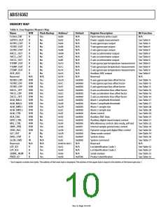
ADIS16362
MEMORY MAP
Table 8. User Register Memory Map
Name
R/W
Flash Backup
Yes
No
No
No
No
No
No
No
No
No
No
No
Address1
0x00
0x02
0x04
0x0ꢃ
0x08
0x0A
0x0C
0x0E
0x±0
0x±2
0x±4
0x±ꢃ
0x±8
0x±A
0x±C
0x±E
0x20
0x22
0x24
0x2ꢃ
0x28
0x2A
0x2C
0x2E
0x30
0x32
0x34
0x3ꢃ
0x38
0x3A
0x3C
0x3E
0x40 to 0xꢀ±
0xꢀ2
0xꢀ4
0xꢀꢃ
0xꢀ8
Default
N/A
N/A
N/A
N/A
N/A
N/A
N/A
N/A
Register Description
Bit Function
N/A
FLASH_CNT
SUPPLY_OUT
XGYRO_OUT
YGYRO_OUT
ZGYRO_OUT
XACCL_OUT
YACCL_OUT
ZACCL_OUT
XTEMP_OUT
YTEMP_OUT
ZTEMP_OUT
AUX_ADC
R
R
R
R
R
R
R
R
R
R
R
R
Flash memory write count
Power supply measurement
X-axis gyroscope output
Y-axis gyroscope output
Z-axis gyroscope output
X-axis accelerometer output
Y-axis accelerometer output
Z-axis accelerometer output
See Table 9
See Table 9
See Table 9
See Table 9
See Table 9
See Table 9
See Table 9
N/A
X-axis gyroscope temperature measurement See Table 9
N/A
N/A
N/A
N/A
Y-axis gyroscope temperature measurement
Z-axis gyroscope temperature measurement
Auxiliary ADC output
See Table 9
See Table 9
See Table 9
N/A
Reserved
N/A
R/W
R/W
R/W
R/W
R/W
R/W
R/W
R/W
R/W
R/W
R/W
R/W
R/W
R/W
R/W
R/W
W
N/A
Yes
Yes
Yes
Yes
Yes
Yes
Yes
Yes
Yes
Yes
Yes
No
Reserved
XGYRO_OFF
YGYRO_OFF
ZGYRO_OFF
XACCL_OFF
YACCL_OFF
ZACCL_OFF
ALM_MAG±
ALM_MAG2
ALM_SMPL±
ALM_SMPL2
ALM_CTRL
AUX_DAC
GPIO_CTRL
MSC_CTRL
SMPL_PRD
SENS_AVG
SLP_CNT
0x0000
0x0000
0x0000
0x0000
0x0000
0x0000
0x0000
0x0000
0x0000
0x0000
0x0000
0x0000
0x0000
0x000ꢃ
0x000±
0x0402
0x0000
0x0000
0x0000
N/A
X-axis gyroscope bias offset factor
Y-axis gyroscope bias offset factor
Z-axis gyroscope bias offset factor
X-axis acceleration bias offset factor
Y-axis acceleration bias offset factor
Z-axis acceleration bias offset factor
Alarm ± amplitude threshold
Alarm 2 amplitude threshold
Alarm ± sample size
Alarm 2 sample size
Alarm control
Auxiliary DAC data
Auxiliary digital input/output control
Miscellaneous control: data ready, self-test
Internal sample period (rate) control
Dynamic range and digital filter control
Sleep mode control
See Table ±ꢀ
See Table ±ꢀ
See Table ±ꢀ
See Table ±ꢃ
See Table ±ꢃ
See Table ±ꢃ
See Table 2ꢁ
See Table 2ꢁ
See Table 28
See Table 28
See Table 29
See Table 23
See Table 2±
See Table 22
See Table ±8
See Table 20
See Table ±9
See Table 2ꢃ
See Table ±ꢁ
N/A
No
Yes
Yes
Yes
No
DIAG_STAT
GLOB_CMD
Reserved
LOT_ID±
LOT_ID2
R
W
N/A
R
R
No
System status
System command
Reserved
N/A
N/A
Yes
Yes
Yes
Yes
N/A
N/A
N/A
0x3F8ꢃ
Lot Identification Code ±
Lot Identification Code 2
Serial number
See Table 32
See Table 32
See Table 32
See Table 32
SERIAL_NUM
PROD_ID
R
R
Product identification
± Each register contains two bytes. The address of the lower byte is displayed. The address of the upper byte is equal to the address of the lower byte plus ±.
Rev. 0 | Page ±0 of 20

 ADI [ ADI ]