ADG406/ADG407/ADG426
TERMINOLOGY
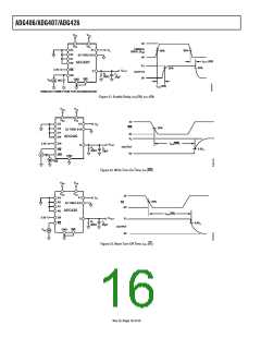
t
OFF (EN)
VDD
Delay time between the 50% and 90% points of the digital input
and switch off condition.
Most positive power supply potential.
VSS
tTRANSITION
Most negative power supply potential in dual supplies. In single
supply applications, it may be connected to ground.
Delay time between the 50% and 90% points of the digital
inputs and the switch on condition when switching from
one address state to another.
GND
Ground (0 V) reference.
tOPEN
RON
Off time measured between 80% points of both switches when
switching from one address state to another.
Ohmic resistance between the D and S terminals.
RON Match
VINL
Difference between the RON of any two channels.
Maximum input voltage for Logic 0.
IS (Off)
VINH
Source leakage current when the switch is off.
Minimum input voltage for Logic 1.
ID (Off)
IINL (IINH)
Drain leakage current when the switch is off.
Input current of the digital input.
ID, IS (On)
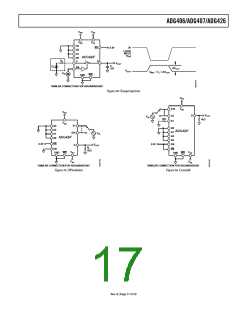
Crosstalk
Channel leakage current when the switch is on.
A measure of unwanted signal which is coupled through from
one channel to another as a result of parasitic capacitance.
VD (VS)
Analog voltage on Terminal D, Terminal S.
Off Isolation
A measure of unwanted signal coupling through an off channel.
CS (Off)
Channel input capacitance for off condition.
Charge Injection
A measure of the glitch impulse transferred from the digital
input to the analog output during switching.
CD (Off)
Channel output capacitance for off condition.
IDD
CD, CS (ON)
Positive supply current.
On switch capacitance.
ISS
CIN
Negative supply current.
Digital input capacitance.
t
ON (EN)
Delay time between the 50% and 90% points of the digital input
and switch on condition.
Rev. B | Page 18 of 20

 ADI [ ADI ]