Data Sheet
ADA4627-1/ADA4637-1
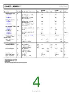
ABSOLUTE MAXIMUM RATINGS
Table 3.
THERMAL RESISTANCE
θJA is specified for the worst-case conditions, that is, a device
soldered in a circuit board for surface-mount packages. This
was measured using a standard 2-layer board. For the LFCSP
package, the exposed pad should be soldered to a copper plane.
Parameter
Rating
Supply Voltage
Input Voltage Range1
Input Current1
Differential Input Voltage2
Output Short-Circuit Duration to GND Indefinite
Storage Temperature Range
Operating Temperature Range
Junction Temperature Range
36 V
(V−) − 0.3 V to (V+) + 0.3 V
10 mA
VSY
Table 4. Thermal Resistance
Package Type
θJA
155
77
θJC
45
14
Unit
°C/W
°C/W
−65°C to +150°C
−40°C to +125°C
−65°C to +150°C
8-Lead SOIC_N (R-8)
8-Lead LFCSP (CP-8-2)
Lead Temperature (Soldering, 60 sec) 300°C
ESD Human Body Model 4 kV
ESD CAUTION
1 Input pin has clamp diodes to the power supply pins. Input current should
be limited to 10 mA or less whenever input signals exceed the power supply
rail by 0.3 V.
2 Differential input voltage is limited to 30 V or the supply voltage, whichever
is less.
Stresses above those listed under Absolute Maximum Ratings
may cause permanent damage to the device. This is a stress
rating only; functional operation of the device at these or any
other conditions above those indicated in the operational
section of this specification is not implied. Exposure to absolute
maximum rating conditions for extended periods may affect
device reliability.
Rev. E | Page 5 of 20

 ADI [ ADI ]