AD8615/AD8616/AD8618
APPLICATIONS
This reduces the overshoot and minimizes ringing, which
in turn improves the frequency response of the AD8615/
AD8616/AD8618. One simple technique for compensation is
the snubber, which consists of a simple RC network. With this
circuit in place, output swing is maintained and the amplifier
is stable at all gains.
INPUT OVERVOLTAGE PROTECTION
The AD8615/AD8616/AD8618 have internal protective cir-
cuitry that allows voltages exceeding the supply to be applied
at the input.
It is recommended, however, not to apply voltages that exceed
the supplies by more than 1.5 V at either input of the amplifier.
If a higher input voltage is applied, series resistors should be
used to limit the current flowing into the inputs.
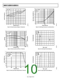
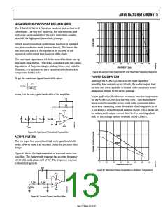
Figure 38 shows the implementation of the snubber, which
reduces overshoot by more than 30% and eliminates ringing
that can cause instability. Using the snubber does not recover
the loss of bandwidth incurred from a heavy capacitive load.
The input current should be limited to <5 mA. The extremely
low input bias current allows the use of larger resistors, which
allows the user to apply higher voltages at the inputs. The use
of these resistors adds thermal noise, which contributes to the
overall output voltage noise of the amplifier.
V
A
C
= ±2.5V
= 1
= 500pF
S
V
L
For example, a 10 kΩ resistor has less than 13 nV/√Hz of
thermal noise and less than 10 nV of error voltage at room
temperature.
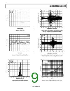
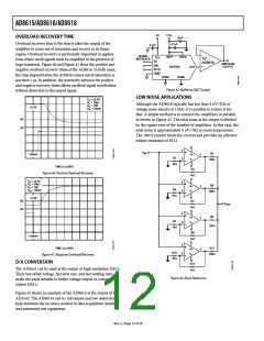
OUTPUT PHASE REVERSAL
The AD8615/AD8616/AD8618 are immune to phase
inversion, a phenomenon that occurs when the voltage
applied at the input of the amplifier exceeds the maxi-
mum input common mode.
TIME (2μs/DIV)
Phase reversal can cause permanent damage to the ampli-
fier and can create lock-ups in systems with feedback loops.
Figure 37. Driving Heavy Capacitive Loads Without Compensation
V
V
A
R
= ±2.5V
S
V
CC
= 6V p-p
= 1
IN
V
L
= 10kΩ
+
–
V–
V+
200Ω
500pF
+
–
500pF
V
EE
200mV
V
OUT
V
IN
Figure 38. Snubber Network
V
= ±2.5V
= 1
S
A
R
C
C
V
S
S
L
= 200
Ω
= 500pF
= 500pF
TIME (2ms/DIV)
Figure 36. No Phase Reversal
DRIVING CAPACITIVE LOADS
Although the AD8615/AD8616/AD8618 are capable of driving
capacitive loads of up to 500 pF without oscillating, a large
amount of overshoot is present when operating at frequencies
above 100 kHz. This is especially true when the amplifier is
configured in positive unity gain (worst case). When such large
capacitive loads are required, the use of external compensation
is highly recommended.
TIME (10μs/DIV)
Figure 39. Driving Heavy Capacitive Loads Using the Snubber Network
Rev. C | Page 11 of 20

 ADI [ ADI ]