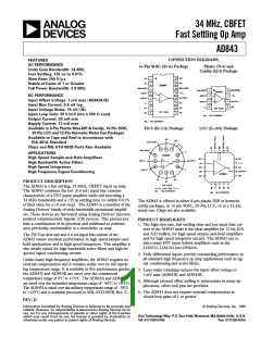
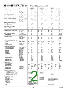
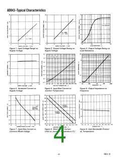
AD843
NOTES
1Standard Military Drawings Available: 5962-9098001M2A (SE/883B), 5962-9098001MXA (SH/883B), 5962-9098001MPA (SQ/883B).
2Specifications are guaranteed after 5 minutes at TA = +25°C.
3Full power bandwidth = Slew Rate/2 πV peak.
4All “S” grade TMIN-TMAX specifications are tested with automatic test equipment at TA = –55°C and TA = +125°C.
Specifications subject to change without notice.
Specifications in boldface are tested on all production units at final electrical test. Results from those tests are used to calculate outgoing quality levels. All min and
max specifications are guaranteed although only those shown in boldface are tested on all production units.
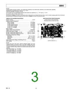
ABSOLUTE MAXIMUM RATINGS1
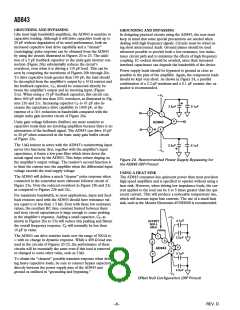
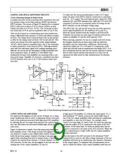
METALIZATION PHOTOGRAPH
Contact factory for latest dimensions.
Dimensions shown in inches and (mm).
Supply Voltage . . . . . . . . . . . . . . . . . . . . . . . . . . . . . . . . .±18 V
Internal Power Dissipation2
Plastic Package . . . . . . . . . . . . . . . . . . . . . . . . . . 1.50 Watts
Cerdip Package . . . . . . . . . . . . . . . . . . . . . . . . . 1.35 Watts
12-Pin Header Package . . . . . . . . . . . . . . . . . . . 1.80 Watts
16-Pin SOIC Package . . . . . . . . . . . . . . . . . . . . 1.50 Watts
20-Pin LCC Package . . . . . . . . . . . . . . . . . . . . . . 1.00 Watt
Input Voltage . . . . . . . . . . . . . . . . . . . . . . . . . . . . . . . . . . ±VS
Output Short Circuit Duration . . . . . . . . . . . . . . . . Indefinite
Differential Input Voltage . . . . . . . . . . . . . . . . . . +VS and –VS
Storage Temperature Range (N, R) . . . . . . . –65°C to +125°C
Storage Temperature Range (Q, H, E) . . . . –65°C to +150°C
Operating Temperature Range
AD843J/R . . . . . . . . . . . . . . . . . . . . . . . . . . . 0°C to +70°C
AD843A/B . . . . . . . . . . . . . . . . . . . . . . . . . –40°C to +85°C
AD843S . . . . . . . . . . . . . . . . . . . . . . . . . . –55°C to +125°C
Lead Temperature Range (Soldering 60 sec) . . . . . . . . +300°C
ESD Rating . . . . . . . . . . . . . . . . . . . . . . . . . . . . . . . . . . 500 V
NOTES
1Stresses above those listed under “Absolute Maximum Ratings” may cause
permanent damage to the device at these or any other conditions above those
indicated in the operational sections of this specification is not implied. Exposure
to absolute maximum rating conditions for extended periods may affect device
reliability.
28-Pin Plastic Package: θJA = 100°C/Watt
8-Pin Cerdip Package: θJA = 110°C/Watt
12-Pin Header Package: θJA = 80°C/Watt
16-Pin SOIC Package: θJA = 100°C/Watt
20-Pin LCC Package: θJA = 150°C/Watt
REV. D
–3–

 ADI [ ADI ]