AD8307
Note that only two design parameters are involved in determin-
ing VY, namely, the cell gain A and the knee voltage EK, while
N, the number of stages, is unimportant in setting the slope of
the overall function. For A = 5 and EK = 100 mV, the slope
would be a rather awkward 572.3 mV per decade (28.6 mV/dB).
A well designed log amp will have rational scaling parameters.
A EK
log10
VY
=
(6)
A
(
)
Preference for the A/0 style of log amp, over one using A/1 cells,
stems from several considerations. T he first is that an A/0 cell
can be very simple. In the AD8307 it is based on a bipolar-
transistor differential pair, having resistive loads RL and an
emitter current source, IE. T his will exhibit an equivalent knee-
voltage of EK = 2 kT /q and a small signal gain of A = IERL /EK.
T he large signal transfer function is the hyperbolic tangent (see
dotted line in Figure 23). T his function is very precise, and the
deviation from an ideal A/0 form is not detrimental. In fact, the
rounded shoulders of the tanh function beneficially result in a
lower ripple in the logarithmic conformance than that obtained
using an ideal A/0 function.
T he intercept voltage can be determined by using two pairs of
transition points on the output function (consider Figure 22).
T he result is:
EK
VX
=
(5)
N +1/ A−1
(
)
)
A(
For the case under consideration, using N = 6, we calculate
VZ = 4.28 µV. However, we need to be careful about the inter-
pretation of this parameter, since it was earlier defined as the
input voltage at which the output passes through zero (see Fig-
ure 19). But clearly, in the absence of noise and offsets, the
output of the amplifier chain shown in Figure 21 can be zero
when, and only when, VIN = 0. T his anomaly is due to the finite
gain of the cascaded amplifier, which results in a failure to maintain
the logarithmic approximation below the lin-log transition (point ➀
in Figure 22). Closer analysis shows that the voltage given by
Equation 5 represents the extrapolated, rather than actual,
intercept.
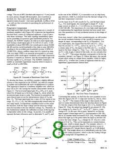
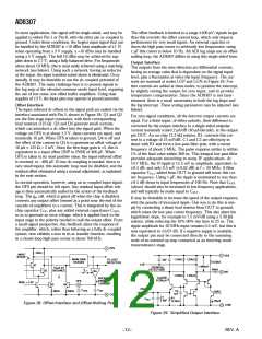
An amplifier built of these cells is entirely differential in struc-
ture and can thus be rendered very insensitive to disturbances
on the supply lines and, with careful design, to temperature
variations. T he output of each gain cell has an associated
transconductance (gm) cell, which converts the differential out-
put voltage of the cell to a pair of differential currents, which are
summed simply by connecting the outputs of all the gm (detec-
tor) stages in parallel. T he total current is then converted back
to a voltage by a transresistance stage, to generate the logarith-
mic output. T his scheme is depicted, in single-sided form, in
Figure 24.
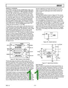
D em odulating Log Am ps
Log amps based on a cascade of A/1 cells are useful in baseband
applications, because they do not demodulate their input signal.
However, baseband and demodulating log amps alike can be
made using a different type of amplifier stage, which we will call
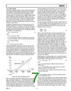
an A/0 cell. Its function differs from that of the A/1 cell in that
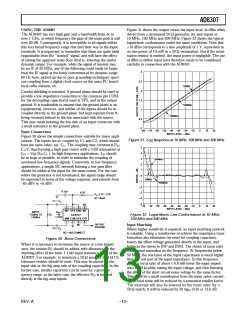
the gain above the knee voltage EK falls to zero, as shown by the
solid line in Figure 23. T his is also known as the limiter func-
tion, and a chain of N such cells is often used to generate a
hard-limited output, in recovering the signal in FM and PM
modes.
2
3
4
AV
A V
A V
A V
IN
IN
IN
IN
A/0
A/0
A/0
A/0
V
V
LIM
IN
g
g
g
g
g
m
m
m
m
m
I
OUT
Figure 24. Log Am p Using A/0 Stages and Auxiliary Sum -
m ing Cells
T he chief advantage of this approach is that the slope voltage
may now be decoupled from the knee-voltage EK = 2 kT /q,
which is inherently PT AT . By contrast, the simple summation
of the cell outputs would result in a very high temperature coef-
ficient of the slope voltage given by Equation 6. T o do this, the
detector stages are biased with currents (not shown in the Fig-
ure) which are rendered stable with temperature. T hese are
derived either from the supply voltage (as in the AD606 and
AD608) or from an internal bandgap reference (as in the AD640
and AD8307). T his topology affords complete control over the
magnitude and temperature behavior of the logarithmic slope,
decoupling it completely from EK.
SLOPE = 0
AE
K
TANH
A/0
SLOPE = A
0
E
K
INPUT
Figure 23. A/0 Am plifier Functions (Ideal and Tanh)
The AD640, AD606, AD608, AD8307 and various other Analog
Devices communications products incorporating a logarithmic
IF amplifier all use this technique. It will be apparent that the
output of the last stage can no longer provide the logarithmic
output, since this remains unchanged for all inputs above the
limiting threshold, which occurs at VIN = EK /AN–1. Instead, the
logarithmic output is now generated by summing the outputs of
all the stages. T he full analysis for this type of log amp is only
slightly more complicated than that of the previous case. It is
readily shown that, for practical purpose, the intercept voltage
VX is identical to that given in Equation 5, while the slope
voltage is:
A further step is yet needed to achieve the demodulation response,
required when the log amp is to convert an alternating input
into a quasi-dc baseband output. T his is achieved by altering the
gm cells used for summation purposes to also implement the
rectification function. Early discrete log amps based on the
progressive compression technique used half-wave rectifiers.
T his made post-detection filtering difficult. T he AD640 was the
first commercial monolithic log amp to use a full-wave rectifier,
a practice followed in all subsequent Analog Devices types.
REV. A
–9–

 ADI [ ADI ]