AD8307
*Stresses above those listed under Absolute Maximum Ratings may cause perma-
nent damage to the device. T his is a stress rating only; functional operation of the
device at these or any other conditions above those indicated in the operational
section of this specification is not implied. Exposure to absolute maximum rating
conditions for extended periods may effect device reliability.
ABSO LUTE MAXIMUM RATINGS*
Supply Voltage . . . . . . . . . . . . . . . . . . . . . . . . . . . . . . . +7.5 V
Input Voltage (Pins 1, 8) . . . . . . . . . . . . . . . . . . . . . . VSUPPLY
Storage T emperature Range, N, R . . . . . . . . –65°C to +125°C
Ambient T emperature Range, Rated Performance Industrial,
AD8307AN, AD8307AR . . . . . . . . . . . . . –40°C to +85°C
Lead T emperature Range (Soldering 10 sec) . . . . . . . +300°C
O RD ERING GUID E
Model
Tem perature Range
P ackage D escriptions
P ackage O ptions
AD8307AR
AD8307AN
AD8307AR-REEL
AD8307AR-REEL7
AD8307-EB
–40°C to +85°C
–40°C to +85°C
SOIC
SO-8
N-8
Plastic DIP
13" REEL
7" REEL
Evaluation Board
CAUTIO N
ESD (electrostatic discharge) sensitive device. Electrostatic charges as high as 4000 V readily
accumulate on the human body and test equipment and can discharge without detection. Although
the AD8307 features proprietary ESD protection circuitry, permanent damage may occur on
devices subjected to high energy electrostatic discharges. T herefore, proper ESD precautions are
recommended to avoid performance degradation or loss of functionality.
WARNING!
ESD SENSITIVE DEVICE
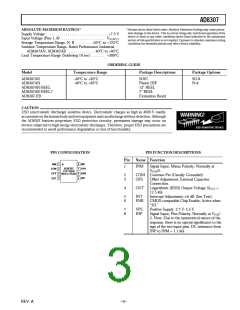
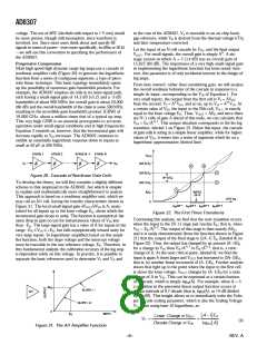
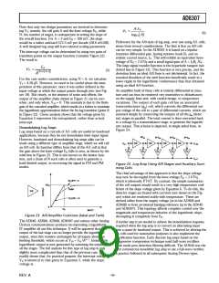
P IN CO NFIGURATIO N
P IN FUNCTIO N D ESCRIP TIO NS
Nam e Function
P in
1
2
3
4
8
7
6
5
INP
INM
COM
OFS
1
INM
Signal Input, Minus Polarity; Normally at
POS/2.
AD8307
TOP VIEW
(Not to Scale)
VPS
ENB
INT
V
2
3
COM
OFS
Common Pin (Usually Grounded).
Offset Adjustment; External Capacitor
Connection.
OUT
4
OUT
Logarithmic (RSSI) Output Voltage; ROUT
12.5 kΩ.
=
5
6
INT
ENB
Intercept Adjustment; ±6 dB (See T ext).
CMOS-compatible Chip Enable; Active when
“HI.”
7
8
VPS
INP
Positive Supply, 2.7 V–5.5 V.
Signal Input, Plus Polarity; Normally at VPOS
/
2. Note: Due to the symmetrical nature of the
response, there is no special significance to the
sign of the two input pins. DC resistance from
INP to INM = 1.1 kΩ.
REV. A
–3–

 ADI [ ADI ]