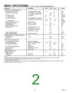
(V = +5 V, T = 25؇C, R ≥ 1 M⍀, unless otherwise noted)
AD8307–SPECIFICATIONS
S
A
L
P aram eter
Conditions
Min
Typ
Max
Units
GENERAL CHARACT ERIST ICS
Input Range (±1 dB Error)
Logarithmic Conformance
Expressed in dBm re 50 Ω
f ≤ 100 MHz, Central 80 dB
f = 500 MHz, Central 75 dB
Unadjusted1
–72
16
±1
dBm
dB
dB
mV/dB
mV/dB
µV
±0.3
±0.5
25
Logarithmic Slope
vs. T emperature
Logarithmic Intercept
23
23
27
27
Sine Amplitude; Unadjusted2
20
Equivalent Sine Power in 50 Ω
–87
–88
–84
–77
–76
dBm
dBm
nV/√Hz
dBm
kΩ
vs. T emperature
Input Noise Spectral Density
Operating Noise Floor
Output Resistance
Inputs Shorted
RSOURCE = 50 Ω/2
Pin 4 to Ground
1.5
–78
12.5
3.5
10
15
Internal Load Capacitance
Response T ime
pF
Small Signal, 10%-90%,
0 mV–100 mV, CL = 2 pF
Large Signal, 10%-90%,
0 V–2.4 V, CL = 2 pF
400
ns
500
ns
Upper Usable Frequency3
Lower Usable Frequency
500
10
MHz
Hz
Input AC-Coupled
–3 dB
AMPLIFIER CELL CHARACT ERIST ICS
Cell Bandwidth
Cell Gain
900
14.3
MHz
dB
INPUT CHARACT ERIST ICS
DC Common-Mode Voltage
Common-Mode Range
Inputs AC-Coupled
Either Input (Small Signal)
RSOURCE ≤ 50 Ω
Drift
Differential
Either Pin to Ground
Either Input
3.2
1.6
50
0.8
1.1
1.4
10
V
V
µV
µV/°C
kΩ
pF
–0.3
VS – 1
500
DC Input Offset Voltage4
Incremental Input Resistance
Input Capacitance
Bias Current
25
µA
POWER INT ERFACES
Supply Voltage
Supply Current
Disabled
2.7
5.5
10
750
V
mA
µA
VENB ≥ 2 V
VENB ≤ 1 V
8
150
NOT ES
1T his may be adjusted downward by adding a shunt resistor from the Output to Ground. A 50 k Ω resistor will reduce the nominal slope to 20 mV/dB.
2T his may be adjusted in either direction by a voltage applied to Pin 5, with a scale factor of 8 dB/V.
3See Application on 900 MHz operation.
4Normally nulled automatically by internal offset correction loop. May be manually nulled by a voltage applied between Pin 3 and Ground; see APPLICAT IONS.
Specifications subject to change without notice.
–2–
REV. A

 ADI [ ADI ]