AD8307
In most applications, the signal will be single-sided, and may be
applied to either Pin 1 or Pin 8, with the other pin ac-coupled to
ground. Under these conditions, the largest input signal that can
be handled by the AD8307 is +10 dBm (sine amplitude of ±1 V)
when operating from a 3 V supply; a +16 dBm may be handled
using a 5 V supply. T he full 16 dBm may be achieved for sup-
plies down to 2.7 V, using a fully balanced drive. For frequencies
above about 10 MHz, this is most easily achieved using a matching
network (see below). Using such a network, having an inductor
at the input, the input transient noted above is eliminated. Occa-
sionally, it may be desirable to use the dc-coupled potential of
the AD8307. T he main challenge here is to present signals to
the log amp at the elevated common-mode input level, requiring
the use of low noise, low offset buffer amplifiers. Using dual
supplies of ±3 V, the input pins may operate at ground potential.
T he offset feedback is limited to a range ±400 µV; signals larger
than this override the offset control loop, which only impacts
performance for very small inputs. An external capacitor re-
duces the high pass corner to arbitrarily low frequencies; using
1 µF this corner is below 10 Hz. All ADI log amps use an offset-
nulling loop; the AD8307 differs in using this single-sided form.
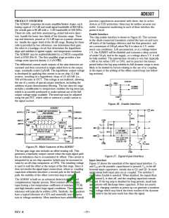
O utput Inter face
T he outputs from the nine detectors are differential currents,
having an average value that is dependent on the signal input
level, plus a fluctuation at twice the input frequency. T he cur-
rents are summed at nodes LGP and LGN in Figure 29. Fur-
ther currents are added at these nodes, to position the intercept,
by slightly raising the output for zero input, and to provide
temperature compensation. Since the AD8307 is not laser-
trimmed, there is a small uncertainty in both the log slope and
the log intercept. T hese scaling parameters may be adjusted (see
below).
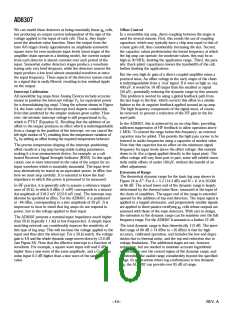
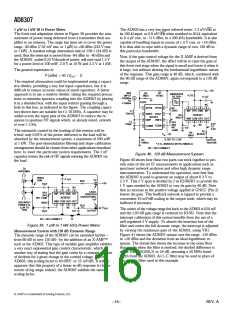
O ffset Inter face
T he input-referred dc offsets in the signal path are nulled via the
interface associated with Pin 3, shown in Figure 28. Q1 and Q2
are the first stage input transistors, with their corresponding
load resistors (125 Ω). Q3 and Q4 generate small currents,
which can introduce a dc offset into the signal path. When the
voltage on OFS is at about 1.5 V, these currents are equal, and
nominally 16 µA. When OFS is taken to ground, Q4 is off and
the effect of the current in Q3 is to generate an offset voltage of
16 µA × 125 Ω = 2 mV. Since the first stage gain is ×5, this is
equivalent to a input offset (INP to INM) of 400 µV. When
OFS is taken to its most positive value, the input-referred offset
is reversed, to –400 µV. If true dc-coupling is needed, down to
very small inputs, this automatic loop must be disabled, and the
residual offset eliminated using a manual adjustment, as explained
in the next section.
For zero-signal conditions, all the detector output currents are
equal. For a finite input, of either polarity, their difference is
converted by the output interface to a single-sided unipolar
current nominally scaled 2 µA/dB (40 µA/decade), at the output
pin OUT . An on-chip 12.5 kΩ resistor, R1, converts this cur-
rent to a voltage of 25 mV/dB. C1 and C2 are effectively in
shunt with R1 and form a low-pass filter pole, with a corner
frequency of about 5 MHz. T he pulse response settles to within
1% of the final value within 300 ns. T his integral low-pass filter
provides adequate smoothing in many IF applications. At
10.7 MHz, the 2f ripple is 12.5 mV in amplitude, equivalent to
±0.5 dB, and only 0.5 mV (±0.02 dB) at f = 50 MHz. A filter
capacitor CFLT added from OUT to ground will lower this cor-
ner frequency. Using 1 µF, the ripple is maintained to less than
±0.5 dB down to input frequencies of 100 Hz. Note that COFS
(above) should also be increased in low frequency applications,
In normal operation, however, using an ac-coupled input signal,
the OFS pin should be left open. Any residual input-offset volt-
age is then automatically nulled by the action of the feedback
loop. T he gm cell, which is gated off when the chip is disabled,
converts any output offset (sensed at a point near the end of the
cascade of amplifiers) to a current. T his is integrated by the on-
and will typically be made equal to CFLT
.
It may be desirable to increase the speed of the output response,
with the penalty of increased ripple. One way to do this is sim-
ply by connecting a shunt load resistor from OUT to ground,
which raises the low pass corner frequency. T his also alters the
logarithmic slope, for example to 7.5 mV/dB using a 5.36 kΩ
resistor, while reducing the 10%-90% rise time to 25 ns. T he
ripple amplitude for 50 MHz input remains 0.5 mV, but this is
now equivalent to ±0.07 dB. If a negative supply is available,
the output pin may be connected directly to the summing
node of an external op amp connected as an inverting-mode
transresistance stage.
chip capacitor CHP, plus any added external capacitance COFS
,
so as to generate an error voltage, which is applied back to the
input stage in the polarity needed to null the output offset. From
a small-signal perspective, this feedback alters the response of
the amplifier, which, rather than behaving as a fully dc-coupled
system, now exhibits a zero in its ac transfer function, resulting
in a closed-loop high-pass corner at about 700 kHz.
VPS
125⍀
INPUT
STAGE
VPS
MAIN GAIN
TO LAST
1.25k⍀ 1.25k⍀
1.25k⍀ 1.25k⍀
3pF
FROM ALL
8.25k⍀
60k⍀
STAGES
DETECTOR
LGP
LGM
Q1
400mV
16A AT
BALANCE
S
DETECTORS
Q2
g
m
INT
2A/dB
0-220A
AVERAGE
ERROR
CURRENT
OFS
BIAS, 1.2V
Q3
36k⍀
Q4
25mV/dB
OUT
C
C
HP
OFS
48k⍀
C2
1pF
BIAS
COM
C1
2.5pF
R1
12.5k⍀
C
FLT
60A
Figure 28. Offset Interface and Offset-Nulling Path
COM
Figure 29. Sim plified Output Interface
REV. A
–12–

 ADI [ ADI ]