AD8307
P RO D UCT O VERVIEW
junction capacitances associated with them, due to active
devices or ESD protection; these may be neither accurate nor
stable. Component numbering in each of these interface dia-
grams is local.
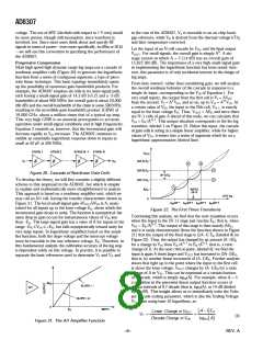
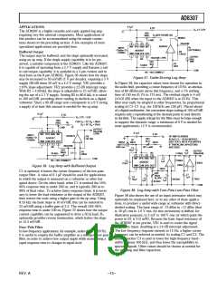
T he AD8307 comprises six main amplifier/limiter stages, each
having a gain of 14.3 dB and small signal bandwidth of 900 MHz;
the overall gain is 86 dB with a –3 dB bandwidth of 500 MHz.
T hese six cells, and their associated gm-styled full-wave detec-
tors, handle the lower two-thirds of the dynamic range. T hree
top-end detectors, placed at 14.3 dB taps on a passive attenua-
tor, handle the upper third of the 90 dB range. Biasing for these
cells is provided by two references: one determines their gain;
the other is a bandgap circuit that determines the logarithmic
slope and stabilizes it against supply- and temperature-variations.
T he AD8307 may be enabled/disabled by a CMOS-compatible
level at ENB (Pin 6). T he first amplifier stage provides a low
voltage noise spectral density (1.5 nV/√Hz).
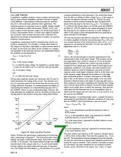
Enable Inter face
T he chip-enable interface is shown in Figure 26. T he currents
in the diode-connected transistors control the turn-on and turn-
off states of the bandgap reference and the bias generator, and
are a maximum of 100 µA when Pin 6 is taken to 5 V, under
worst case conditions. Left unconnected, or at a voltage below
1 V, the AD8307 will be disabled and consume a sleep current
of under 50 µA; tied to the supply, or a voltage above 2 V, it will
be fully enabled. T he internal bias circuitry is very fast (typically
<100 ns for either OFF or ON), and in practice the latency
period before the log amp exhibits its full dynamic range is more
likely to be limited by factors relating to the use of ac coupling
at the input or the settling of the offset-control loop (see follow-
ing sections).
T he differential current-mode outputs of the nine detectors are
summed and then converted to single-sided form in the output
stage, nominally scaled 2 µA/dB. T he logarithmic output voltage
is developed by applying this current to an on-chip 12.5 kΩ
resistor, resulting in a logarithmic slope of 25 mV/dB (i.e.,
500 mV/decade) at OUT . T his voltage is not buffered, allowing
the use of a variety of special output interfaces, including the
addition of post-demodulation filtering. T he last detector stage
includes a modification to temperature-stabilize the log intercept,
which is accurately positioned to make optimal use of the full
output voltage range available. T he intercept may be adjusted
using the pin INT , which adds or subtracts a small current to
the signal current.
AD8307
40k⍀
ENB
TO BIAS
STAGES
COM
Figure 26. Enable Interface
AD8307
VPS
VPS
ENB
BAND GAP REFERENCE
SUPPLY
7.5mA
ENABLE
INT. ADJ
AND BIASING
S
125⍀
SIX 14.3dB 900MHz
AMPLIFIER STAGES
INT
6k⍀
INP
1.1k⍀
COM
+INPUT
–INPUT
MIRROR
2k⍀
6k⍀
C
P
INM
2A
/dB
3
OUT
Q1
INP
INM
OUTPUT
2
NINE DETECTOR CELLS
SPACED 14.3dB
12.5k⍀
TOP-END
DETECTORS
4k⍀
C
D
~3k⍀
COMMON
COM
COM
Q2
OFS
INPUT– OFFSET
COMPENSATION LOOP
OFS. ADJ.
TYP +2.2V FOR
+3V SUPPLY,
+3.2V AT +5V
C
M
COM
I
E
COM
2.4mA
S
Figure 25. Main Features of the AD8307
T he last gain stage also includes an offset-sensing cell. T his
generates a bipolarity output current when the main signal path
has an imbalance due to accumulated dc offsets. T his current is
integrated by an on-chip capacitor (which may be increased in
value by an off-chip component, at OFS). T he resulting voltage
is used to null the offset at the output of the first stage. Since it
does not involve the signal input connections, whose ac coupling
capacitors otherwise introduce a second pole in the feedback
path, the stability of the offset correction loop is assured.
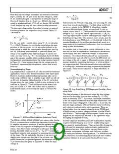
COM
Figure 27. Signal Input Interface
Input Inter face
Figure 27 shows the essentials of the signal input interface. CP
and CM are the parasitic capacitances to ground; CD is the dif-
ferential input capacitance, mostly due to Q1 and Q2. In most
applications both input pins are ac-coupled. T he switches S
close when Enable is asserted. When disabled, the inputs float,
bias current IE is shut off, and the coupling capacitors remain
charged. If the log amp is disabled for long periods, small leak-
age currents will discharge these capacitors. If they are poorly
matched, charging currents at power-up can generate a transient
input voltage which may block the lower reaches of the dynamic
range until it has become much less than the signal.
T he AD8307 is built on an advanced dielectrically-isolated
complementary bipolar process. Most resistors are thin-film
types having a low temperature coefficient of resistance (T CR)
and high linearity under large signal conditions. T heir absolute
tolerance will typically be within ±20%. Similarly, the capacitors
have a typical tolerance of ±15% and essentially zero tempera-
ture or voltage sensitivity. Most interfaces have additional small
REV. A
–11–

 ADI [ ADI ]