AD8307
We can model these detectors as being essentially linear gm cells,
but producing an output current independent of the sign of the
voltage applied to the input of each cell. T hat is, they imple-
ment the absolute-value function. Since the output from the
later A/0 stages closely approximates an amplitude-symmetric
square wave for even moderate input levels (most stages of the
amplifier chain operate in a limiting mode), the current output
from each detector is almost constant over each period of the
input. Somewhat earlier detectors stages produce a waveform
having only very brief dropouts, while the detectors nearest the
input produce a low level almost-sinusoidal waveform at twice
the input frequency. T hese aspects of the detector system result
in a signal that is easily filtered, resulting in low residual ripple
on the output.
O ffset Contr ol
In a monolithic log amp, direct-coupling between the stages is
used for several reasons. First, this avoids the use of coupling
capacitors, which may typically have a chip area equal to that of
a basic gain cell, thus considerably increasing die size. Second,
the capacitor values predetermine the lowest frequency at which
the log amp can operate; for moderate values, this may be as
high as 30 MHz, limiting the application range. T hird, the para-
sitic (back-plate) capacitance lowers the bandwidth of the cell,
further limiting the applications.
But the very high dc gain of a direct-coupled amplifier raises a
practical issue. An offset voltage in the early stages of the chain
is indistinguishable from a ‘real’ signal. If it were as high as, say,
400 µV, it would be 18 dB larger than the smallest ac signal
(50 µV), potentially reducing the dynamic range by this amount.
T his problem is averted by using a global feedback path from
the last stage to the first, which corrects this offset in a similar
fashion to the dc negative feedback applied around an op amp.
T he high frequency components of the signal must, of course,
be removed, to prevent a reduction of the HF gain in the for-
ward path.
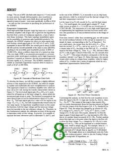
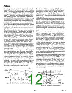
Inter cept Calibr ation
All monolithic log amps from Analog Devices include accurate
means to position the intercept voltage VX (or equivalent power
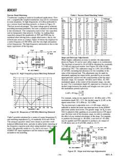
for a demodulating log amp). Using the scheme shown in Figure
24, the basic value of the intercept level departs considerably
from that predicted by the simpler analyses given earlier. How-
ever, the intrinsic intercept voltage is still proportional to EK,
which is PT AT (Equation 5). Recalling that the addition of an
offset to the output produces an effect which is indistinguishable
from a change in the position of the intercept, we can cancel the
left-right motion of VX resulting from the temperature variation of
EK by adding an offset having the required temperature behavior.
In the AD8307, this is achieved by an on-chip filter, providing
sufficient suppression of HF feedback to allow operation above
1 MHz. T o extend the range below this frequency, an external
capacitor may be added. T his permits the high pass corner to be
lowered to audio frequencies using a capacitor of modest value.
Note that this capacitor has no effect on the minimum signal
frequency for input levels above the offset voltage: this extends
down to dc (for a signal applied directly to the input pins). T he
offset voltage will vary from part to part; some will exhibit essen-
tially stable offsets of under 100 µV, without the benefit of an
offset adjustment.
T he precise temperature-shaping of the intercept-positioning
offset results in a log amp having stable scaling parameters,
making it a true measurement device, for example, as a cali-
brated Received Signal Strength Indicator (RSSI). In this appli-
cation, one is more interested in the value of the output for an
input waveform which is invariably sinusoidal. T he input level
may alternatively be stated as an equivalent power, in dBm, but
here we must step carefully. It is essential to know the load
impedance in which this power is presumed to be measured.
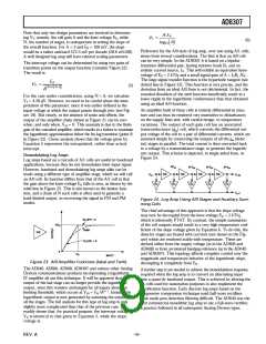
Extension of Range
T he theoretical dynamic range for the basic log amp shown in
Figure 24 is AN. For A = 5.2 (14.3 dB) and N = 6, it is 20,000
or 86 dB. T he actual lower end of the dynamic range is largely
determined by the thermal noise floor, measured at the input of
the chain of amplifiers. T he upper end of the range is extended
upward by the addition of top-end detectors. T he input signal is
applied to a tapped attenuator, and progressively smaller signals
are applied to three passive rectifying gm cells whose outputs are
summed with those of the main detectors. With care in design,
the extension to the dynamic range can be seamless over the full
frequency range. For the AD8307 it amounts to a further 27 dB.
In RF practice, it is generally safe to assume a reference imped-
ance of 50 Ω, in which 0 dBm (1 mW) corresponds to a sinusoi-
dal amplitude of 316.2 mV (223.6 mV rms). T he intercept may
likewise be specified in dBm. For the AD8307, it is positioned
at –84 dBm, corresponding to a sine amplitude of 20 µV. It is
important to bear in mind that log amps do not respond to
power, but to the voltage applied to their input.
T he AD8307 presents a nominal input impedance much higher
than 50 Ω (typically 1.1 kΩ at low frequencies). A simple input
matching network can considerably improve the sensitivity of
this type of log amp. T his will increase the voltage applied to the
input and thus alter the intercept. For a 50 Ω match, the voltage
gain is 4.8 and the whole dynamic range moves down by 13.6 dB
(see Figure 33). Note that the effective intercept is a function of
waveform. For example, a square-wave input will read 6 dB
higher than a sine wave of the same amplitude, and a Gaussian
noise input 0.5 dB higher than a sine wave of the same rms
value.
T he total dynamic range is thus theoretically 113 dB. T he speci-
fied range of 90 dB (–74 dBm to +16 dBm) is that for high
accuracy, calibrated operation, and includes the low end degra-
dation due to thermal noise, and the top end reduction due to
voltage limitations. T he additional stages are not, however,
redundant, but are needed to maintain accurate logarithmic
conformance over the central region of the dynamic range, and
in extending the usable range considerably beyond the specified
range. In applications where log-conformance is less demand-
ing, the AD8307 can provide over 95 dB of range.
REV. A
–10–

 ADI [ ADI ]