High Speed Amplifiers (BW > 50 MHz)
Clamp Amplifiers
AD8036: Low Distortion, Wide Bandwidth Voltage Feedback Clamp Amps
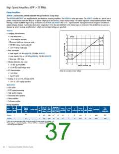
The AD8036 and AD8037 are wide bandwidth, low distortion clamping amplifiers. The AD8036 is unity-gain stable. The AD8037 is stable at a gain of two or
greater. These devices allow the designer to specify a high (VCH) and low (VCL) output clamp voltage. The output signal will clamp at these specified levels.
Utilizing a unique CLAMPIN™ input clamp architecture, the AD8036 and AD8037 offer a 10× improvement in clamp performance compared to traditional
output clamping devices. In particular, clamp error is typically 3 mV or less and distortion in the clamp region is minimized. This product can be used as a
classical op amp or a clamp amplifier where a high and low output voltage are specified.
Features
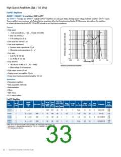
•ꢀClamping characteristics
4
•ꢀ 3 mV clamp error
AD8036
V
= 3V
H
3
2
•ꢀ 1.5 ns overdrive recovery
•ꢀ Minimized nonlinear clamping region
•ꢀ 240 MHz clamp input bandwidth
•ꢀ ±3.9 V clamp input range
V
V
= 2V
= 1V
H
H
1
0
•ꢀWide bandwidth
V
= –1V
= –2V
L
–1
–2
–3
–4
•ꢀ Small signal: 240 MHz (AD8036), 270 MHz (AD8037)
•ꢀ Large signal (4 V p-p): 195 MHz (AD8036), 190 MHz (AD8037)
•ꢀ Slew rate: 1500 V/µs
V
L
V
= –3V
L
•ꢀUltralow distortion, low noise
•ꢀ –72 dBc typ @ 20 MHz
–4
–3
–2
–1
0
1
2
3
4
INPUT VOLTAGE – (V)
•ꢀ 4.5 nV/√Hz input voltage noise
•ꢀDC characteristics
Clamp dc cccuracy vs. input voltage.
•ꢀ 2 mV offset
•ꢀ 10µV/°C drift
•ꢀSettling 10 ns to 0.1%, 16 ns to 0.01%
ꢀ ±3 V to ±5 V supply operation
Applications
• ADC buffer
• IF/RF signal processing
• High quality imaging
• Broadcast video systems
• Video amplifier
• Full wave rectifier
Clamp Amplifiers
Distortion
Supply
Voltage
(V)
BW @ Slew
ACL Min Rate
(MHz) (V/ms)
Price
@ 1k
(OEM $US)
SFDR1 @ BW
Part
Number Amps
No. of
ACL
Min
Noise
(nV/ z)
VOS Max
IB
IS/Amp
IOUT
Temp
Disable
Rail-to-Rail1
Packaging
√H
(mV) (µA Max) (mA Typ) (mA) Range2
(dBc) (MHz)
65
AD8037
AD8036
1
1
2
1
270
1500 –773
1200
–813
10
10
4.5
6.7
7
7
9
18.5
20.5
70
70
I
SOIC
SOIC
4.12
4.28
240
10
H/I
65
1
2
3
RRIO: rail-to-rail input/output, RRO: rail-to-rail output, SS: single supply (IVR includes –VSY).
Temp range: H = extended industrial (–40°C to +125°C), I = industrial (–40°C to +85°C).
THD: total harmonic distortion.
Operational Amplifier Selection Guide
44
|

 ADI [ ADI ]