AD652
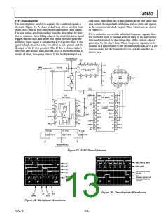
an opto-isolator and latched into a D-flop. The chopper frequency
is generated from an AD654 VFC and is frequency divided by two
to develop differential drive for the chopper transistors, and to
ensure an accurate 50 percent duty cycle. The pull-up resistors
on the D-flop outputs provide a well defined high level voltage
to the choppers to equalize the drive in each direction. The 10 µH
inductor in the +5 V lead of the transformer primary is necessary
to equalize any residual imbalance in the drive on each half-
cycle and thus prevent saturation of the core. The capacitor
across the primary resonates the system so that under light load-
ing conditions on the secondary the wave shape will be sinusoidal
and the clock frequency will be relayed to the SVFC. To adjust
the chopper frequency, disconnect any load on the secondary
and tune the AD654 for a minimum in the supply current drawn
from the 5 volt supply.
Table I.
Conversion
or
Gate Time
Resolution
N
Clock
Typ Lin Comments
12 Bits
12 Bits
12 Bits
4 Digits
14 Bits
14 Bits
14 Bits
4 1/2 Digits 20000
16 Bits
16 Bits
4096
4096
4096
10000
16384
16384
16384
81.92 kHz
2 MHz
4 MHz
100 ms
0.002% 50, 60, 400 Hz NMR
0.01%
0.02%
0.002% 50, 60, 400 Hz NMR
0.002% 50, 60, 400 Hz NMR
4.096 ms
2.048 ms
100 ms
200 kHz
327.68 kHz 100 ms
1.966 MHz 16.66 ms
1.638 MHz 20 ms
0.01%
0.01%
60 Hz NMR
50 Hz NMR
400 kHz
655.36 kHz 200 ms
4 MHz 32.77 ms
100 ms
0.002% 50, 60, 400 Hz NMR
0.002% 50, 60, 400 Hz NMR
0.02%
65536
65536
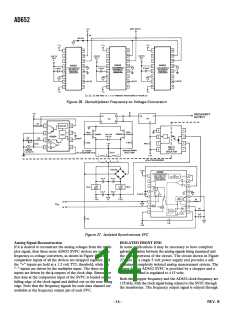
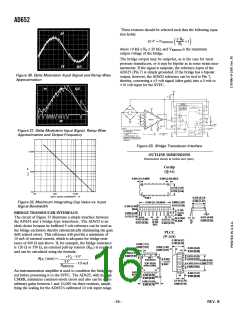
DELTA MODULATOR
The circuit of Figure 29 shows the AD652 configured as a delta
modulator. A reference voltage is applied to the input of the
integrator (Pin 7), which sets the steady state output frequency
at one-half of the AD652 full-scale frequency (1/4 of the clock
frequency). As a 0 V to 10 V input signal is applied to the com-
parator (Pin 15), the output of the integrator attempts to track
this signal. For an input in an idling condition (dc) the output
frequency will be one-half full scale. For positive going signals
the output frequency will be between one-half full scale and full
scale, and for negative going signals the output frequency will be
between zero and one-half full scale. The output frequency will
correspond to the slope of the comparator input signal.
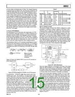
A-TO-D CONVERSION
In performing an A-to-D conversion, the output pulses of a VFC
are counted for a fixed gate interval. To achieve maximum per-
formance with the AD652, the fixed gate interval should be
generated using a multiple of the SVFC clock input. Counting
in this manner will eliminate any errors due to the clock (whether it
be jitter, drift with time or temperature, etc.) since it is the ratio
of the clock and output frequencies that is being measured.
The resolution of the A-to-D conversion measurement is deter-
mined by the clock frequency and the gate time. If, for instance,
a resolution of 12 bits is desired and the clock frequency is 1 MHz
(resulting in an AD652 FS frequency of 500 kHz) the gate time
will be:
–1
–1
1
–1
FS Freq
N
Clock Freq
N
1 MHz
2(4096)
=
=
2
8192
=
sec = 8.192 ms :
Where N is the
total number of
codes for a given
resolution.
1×10⁶
Figure 28 shows the AD652 SVFC as an A-to-D converter in
block diagram form.
Figure 29. Delta Modulator
Since the output frequency corresponds to the slope of the input
signal, the delta modulator acts as a differentiator. A delta modula-
tor is thus a direct way of finding the derivative of a signal. This
is useful in systems where, for example, a signal corresponding
to velocity exists and it is desired to determine acceleration.
Figure 28. Block Diagram of SVFC A-to-D Converter
Figure 30 is a scope photo showing a 20 kHz, 0 V to 10 V sine
wave used as the input to the comparator and its ramp-wise
approximation at the integrator output. The clock frequency used
as 2 MHz and the integrating capacitor was 360 pF. Figure 31
shows the same input signal and its ramp-wise approximation,
along with the output frequency corresponding to the derivative
of the input signal. In this case the clock frequency was 50 kHz.
To provide the ÷ 2N block a single chip counter such as the
4020B can be used. The 4020B is a 14-stage binary ripple
counter which has a clock and master reset for inputs, and buff-
ered outputs from the first stage and the last eleven stages. The
output of the first stage is fCLOCK ÷ 21 = fCLOCK/2) while the
output of the last stage is fCLOCK ÷ 214 = fCLOCK/16384. Hence
using this single chip counter as the ÷ 2N block, 13-bit resolu-
tion can be achieved. Higher resolution can be achieved by
cascading D-type flipflops or another 4020B with the counter.
The choice of an integrating capacitor is primarily dictated by
the input signal bandwidth. Figure 32 shows this relationship. It
should be noted that as the value of CINT is lowered, the ramp
size of the integrator approximation becomes larger. This can
be compensated for by increasing the clock frequency. The effect
of the clock frequency on the ramp size is demonstrated in
Figures 30 and 31.
Table I shows the relationship between clock frequency and gate
time for various degrees of resolution. Note that if the variables
are chosen such that the gate times are multiples of 50 Hz, 60 Hz
or 400 Hz, normal-mode rejection (NMR) of those line fre-
quencies will occur.
REV. B
–15–

 ADI [ ADI ]