AUTOMOTIVE, 125°C OPERATION, 36 V INPUT, 250 mA VOLTAGE REGULATOR
S-19212B/DxxA Series
Rev.5.3_00
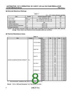
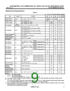
Electrical Characteristics
Table 13
(Tj =
Min.
VOUT(S)
−
40°C to
+
125°C unless otherwise specified)
Test
Item
Symbol
VOUT(E)
Condition
Typ.
Max.
Unit
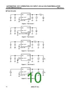
Circuit
VOUT(S)
Output voltage*1
Output current*2
Dropout voltage*3
V
IN = VOUT(S)
+
+
2.0 V, IOUT = 10 mA
2.0 V
VOUT(S)
V
1
×
0.980
250*4
×
1.020
VIN VOUT(S)
≥
−
−
−
−
mA
V
V
3
1
1
IOUT
IOUT = 125 mA, Ta =
IOUT = 250 mA, Ta =
+
+
25°C
25°C
−
−
0.35
0.80
Vdrop
Δ
VOUT1
VOUT(S)
+
0.5 V
≤
VIN
≤
36 V, IOUT = 10 mA
−
−
−
−
−
0.01
16
0.03
%/V
mV
mV
mV
1
1
1
1
2
Line regulation
Δ
VIN
•
VOUT
V
IN = VOUT(S)
+
2.0 V,
<
2.0 V,
<
30
2.5 V
≤
VOUT(S)
5.1 V, 0.1 mA
≤
IOUT
≤
40 mA
40 mA
40 mA
VIN = VOUT(S)
5.1 V VOUT(S)
VIN = VOUT(S)
12.1 V
VIN = 18.0 V,
+
16
35
Load regulation
Δ
VOUT2
≤
12.1 V, 0.1 mA ≤ IOUT ≤
+
2.0 V,
16
40
≤
VOUT(S)
≤
16.0 V, 0.1 mA
≤
IOUT ≤
Current consumption
during operation
Current consumption
during power-off
Input voltage
6.5
8.5
μ
μ
A
A
ISS1
VON / OFF = VIN, IOUT = 0.01 mA
VIN = 18.0 V,
VON / OFF = 0 V, no load
−
−
0.1
−
3.5
36
−
2
−
4
ISS2
VIN
3.0
1.5
V
B type
−
V
V
V
V
V
IN = 18.0 V, RL = 1.0 kΩ,
(ON / OFF logic active "H")
D type
(ON / OFF logic active "H")
B type
(ON / OFF logic active "H")
D type
(ON / OFF logic active "H")
ON / OFF pin
input voltage "H"
determined by VOUT output
level
VSH
2.0
−
−
−
−
−
−
−
4
4
4
4
4
0.25
0.8
0.1
0.1
VIN = 18.0 V, RL = 1.0 kΩ,
determined by VOUT output
level
ON / OFF pin
input voltage "L"
VSL
−
ON / OFF pin
input current "H"
ON / OFF pin
V
V
IN = 18.0 V, VON / OFF = VIN
IN = 18.0 V, VON / OFF = 0 V
−
−
0.1
0.1
μ
A
A
ISH
ISL
μ
input current "L"
2.5 V
3.6 V
≤
≤
VOUT(S)
VOUT(S)
<
<
3.6 V
6.1 V
−
−
45
40
−
−
dB
dB
5
5
VIN = VOUT(S)
f = 100 Hz,
+
2.0 V,
Δ
Vrip = 0.5 Vrms,
Ripple rejection
|RR|
6.1 V
≤
VOUT(S)
<
10.1 V
−
−
35
30
−
−
dB
dB
5
5
IOUT = 10 mA,
Ta = 25°C
+
10.1 V
≤ VOUT(S) ≤ 16.0 V
V
IN = VOUT(S) +
2.0 V,
−
−
−
−
120
165
140
70
−
−
−
−
mA
°C
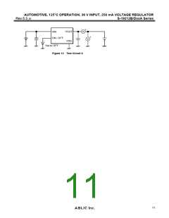
3
−
−
6
Short-circuit current
Ishort
VON / OFF = VIN, VOUT = 0 V, Ta =
+
25°C
Thermal shutdown
detection
temperature
Thermal shutdown
release temperature
Discharge shunt
resistance during
power-off
TSD
Junction temperature
°C
TSR
Junction temperature
V
IN = 18.0 V, VON / OFF = 0 V, VOUT = 2.0 V
kΩ
RLOW
*1. VOUT(S)
:
:
Set output voltage
Actual output voltage
The output voltage when VIN = VOUT(S) + 2.0 V, IOUT = 10 mA
VOUT(E)
*2. The output current at which the output voltage becomes 95% of VOUT(E) after gradually increasing the output current.
*3. Vdrop = VIN1 − (VOUT3 × 0.98)
VIN1 is the input voltage at which the output voltage becomes 98% of VOUT3 after gradually decreasing the input voltage.
VOUT3 is the output voltage when VIN = VOUT(S) + 2.0 V, and IOUT = 125 mA or 250 mA.
*4. Due to limitation of the power dissipation, this value may not be satisfied. Attention should be paid to the power
dissipation when the output current is large.
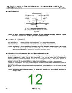
This specification is guaranteed by design.
9

 ABLIC [ ABLIC ]