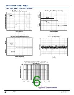
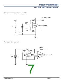
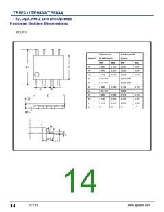
TP5531/TP5532/TP5534
1.8V, 34μA, RRIO, Zero Drift Op-amps
balanced across each input. The input impedance of the amplifier should be matched between the IN+ and IN-
terminals to minimize total input offset current. Input offset currents show up as an additional output offset voltage, as
shown in the following equation:
vos,total vos Rf Ios
For a gain configure using 1Mꢀ feedback resistor, a 150pA total input offset current will have an additional output
offset voltage of 0.15mV. By keeping the input impedance low and balanced across the amplifier inputs, the input
offset current effect will be suppressed efficiently.
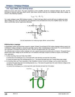
Circuit Implication for reducing Input offset current effect
PCB Surface Leakage
In applications where low input bias current is critical, Printed Circuit Board (PCB) surface leakage effects need to be
considered. Surface leakage is caused by humidity, dust or other contamination on the board. It is recommended to
use multi-layer PCB layout and route the OPA’s -IN and +IN signal under the PCB surface.
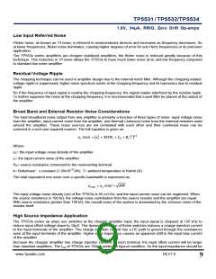
The effective way to reduce surface leakage is to use a guard ring around sensitive pins (or traces). The guard ring is
biased at the same voltage as the sensitive pin. An example of this type of layout is shown in Figure 2 for Inverting
Gain application.
1. For Non-Inverting Gain and Unity-Gain Buffer:
a) Connect the non-inverting pin (VIN+) to the input with a wire that does not touch the PCB surface.
b) Connect the guard ring to the inverting input pin (VIN–). This biases the guard ring to the Common Mode input voltage.
2. For Inverting Gain and Trans-impedance Gain Amplifiers (convert current to voltage, such as photo detectors):
a) Connect the guard ring to the non-inverting input pin (VIN+). This biases the guard ring to the same reference voltage as the
op-amp (e.g., VDD/2 or ground).
b) Connect the inverting pin (VIN–) to the input with a wire that does not touch the PCB surface.
The Layout of Guard Ring
REV1.0
www.3peakic.com
10

 3PEAK [ 3PEAK ]