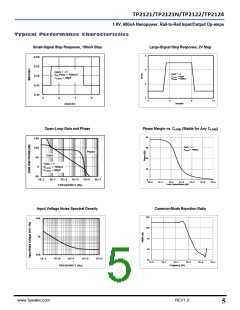
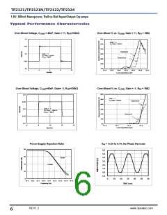
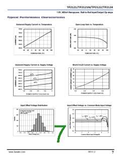
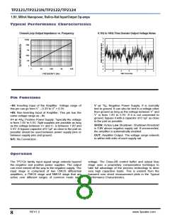
TP2121/TP2121N/TP2122/TP2124
1.8V, 600nA Nanopower, Rail-to-Rail Input/Output Op-amps
Applications Information
Low Supply Voltage and Low Power Consumption
The TP212x family of operational amplifiers can operate with power supply voltages from 1.8V to 6.0V. Each amplifier
draws only 600nA quiescent current. The low supply voltage capability and low supply current are ideal for portable
applications demanding HIGH CAPACITIVE LOAD DRIVING CAPABILITY and CONSTANT WIDE BANDWIDTH. The
TP212x family is optimized for wide bandwidth low power applications. They have an industry leading high GBWP to
power ratio and are unity gain stable for 1,000nF capacitive load. When the load capacitance increases, the increased
capacitance at the output pushed the non-dominant pole to lower frequency in the open loop frequency response,
lowering the phase and gain margin. Higher gain configurations tend to have better capacitive drive capability than
lower gain configurations due to lower closed loop bandwidth and hence higher phase margin.
Low Input Referred Noise
The TP212x family provides a low input referred noise density of 170nV/√Hz at 1kHz. The voltage noise will grow
slowly with the frequency in wideband range, and the input voltage noise is typically 6.5μVP-P at the frequency of 0.1Hz
to 10Hz.
Low Input Offset Voltage
The TP212x family has a low offset voltage of 1.5mV maximum which is essential for precision applications. The offset
voltage is trimmed with a proprietary trim algorithm to ensure low offset voltage for precision signal processing
requirement.
Low Input Bias Current
The TP212x family is a CMOS OPA family and features very low input bias current in pA range. The low input bias
current allows the amplifiers to be used in applications with high resistance sources. Care must be taken to minimize
PCB Surface Leakage. See below section on “PCB Surface Leakage” for more details.
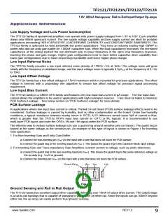
PCB Surface Leakage
In applications where low input bias current is critical, Printed Circuit Board (PCB) surface leakage effects need to be
considered. Surface leakage is caused by humidity, dust or other contamination on the board. Under low humidity
conditions, a typical resistance between nearby traces is 1012Ω. A 5V difference would cause 5pA of current to flow,
which is greater than the TP212x OPA’s input bias current at +27°C (±1fA, typical). It is recommended to use
multi-layer PCB layout and route the OPA’s -IN and +IN signal under the PCB surface.
The effective way to reduce surface leakage is to use a guard ring around sensitive pins (or traces). The guard ring is
biased at the same voltage as the sensitive pin. An example of this type of layout is shown in Figure 1 for Inverting
Gain application.
1. For Non-Inverting Gain and Unity-Gain Buffer:
a) Connect the non-inverting pin (VIN+) to the input with a wire that does not touch the PCB surface.
b) Connect the guard ring to the inverting input pin (VIN–). This biases the guard ring to the Common Mode input voltage.
2. For Inverting Gain and Trans-impedance Gain Amplifiers (convert current to voltage, such as photo detectors):
a) Connect the guard ring to the non-inverting input pin (VIN+). This biases the guard ring to the same reference voltage as
the op-amp (e.g., VDD/2 or ground).
b) Connect the inverting pin (VIN–) to the input with a wire that does not touch the PCB surface.
Figure 1
Ground Sensing and Rail to Rail Output
The TP212x family has excellent output drive capability, delivering over 10mA of output drive current. The output stage
is a rail-to-rail topology that is capable of swinging to within 5mV of either rail. Since the inputs can go 300mV beyond
either rail, the op-amp can easily perform ‘true ground’ sensing.
www.3peakic.com
REV1.2
9

 3PEAK [ 3PEAK ]