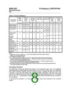
BRIGHT
Microelectronics
Inc.
Preliminary BM29F040
In programming, if the sector being written to is protected, the toggle bit may toggle for about 2 mS
and then will stop toggling without the data being changed. During erase the device will erase all the
sectors except the sector being protected. If all the sectors are protected the chip will toggle the
toggle bit for about 2 mS and then drop back to read mode without changing the data.
Either CE or OE toggling will cause the DQ6 to toggle. The toggle bit is valid in the time out period
during sector erase.
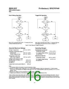
See Figure 13 for the Toggle bit timing diagrams.
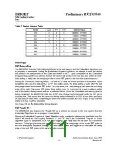
DQ5 Exceeded The Timing Limits
DQ5 indicates if the program or erase time has exceeded the specified timing limits. Under these
conditions DQ5 will produce a "1". This is a failure condition which indicates that the program or erase
cycle was not successfully completed. Data polling is the only operating function of the device under
this condition. The CE circuit will partially power down the device under these conditions. The OE
and WE pins will control the output disable function as shown in Table 4.
If this failure condition occurs during the sector erase operation, it indicates that the particular sector
is bad and may not be reused. The other sectors are still functioning properly and can be used. The
device must be reset to use the other good sectors. To reset the device, write the Reset command
sequence to the device. This will allow the system to use the other active sectors in the device.
If this failure condition occurs during chip erase, it indicates that the entire chip is bad or many sectors
are bad.
If this condition occurs during byte write it indicates that the sector containing this byte is bad.
This failure condition can also occur if the user tries to program a non-blank location without erasing.
In this case the device locks out and never completes the operation. Please note that this is not a
device failure.
DQ3 Sector Erase Timer
After the completion of the Sector erase command sequence the sector erase time-out begins. DQ3
will remain low until the time-out is complete. Data polling and the Toggle bit are valid after the initial
sector erase command sequence.
If Data polling or the Toggle bit indicates the device has been written with a valid erase command,
DQ3 may be used to determine if the sector erase timer window is still open. If DQ3 is "1" the
internally controlled erase cycle has begun. If DQ3 is "0" the device will accept additional sector erase
commands. To ensure that the command has been accepted, the user should check the status of
DQ3 prior to and following each sector erase command. If DQ3 is "1" on the second status check, the
command may not be accepted.
Once the internal erase cycle begins the device will not accept any other command until the internal
erase cycle is completed.
The BM29F040 is designed to offer protection against accidental programming or erasure. During
power-up the device automatically resets to the read mode. The multi-bus command sequences also
provide data protection for accidental write. The device also provides additional features to prevent
inadvertent write operations during power-up and power-down transitions or system noise.
- 12 -

 WINBOND [ WINBOND ]