BCM4414xD1E13A2yzz
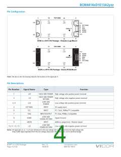
Pin Configuration
10
1
TOP VIEW
3
12
+HI
–HI
–LO
–LO
+LO
5
6
7
8
9
EXT BIAS
SCL
PMBus™
SDA
SGND
ADDR
–LO
–LO
+LO
11
2
4
13
BCM in a 4414 VIA Package - Chassis (Lug) Mount
11
13
2
TOP VIEW
4
–HI
+HI
–LO
–LO
+LO
9
8
7
6
5
ADDR
SGND
SDA
PMBus™
SCL
EXT BIAS
+LO
–LO
–LO
10
1
3
12
BCM in a 4414 VIA Package - Board (PCB) Mount
Note: The dot on the VIA housing indicates the location of the signal pin 9.
Pin Descriptions
Pin Number
Signal Name
Type
Function
1
2
+HI
–HI
HIGH SIDE POWER High voltage side positive power terminal
HIGH SIDE POWER
High voltage side negative power terminal
RETURN
LOW SIDE
3, 4
+LO
Low voltage side positive power terminal
POWER
5
6
7
EXT BIAS
SCL
INPUT
INPUT
5V supply input
I2C Clock, PMBus™ Compatible
I2C Data, PMBus Compatible
SDA
INPUT/OUTPUT
LOW SIDE
SIGNAL RETURN
8
SGND
ADDR
–LO
Signal Ground
9
INPUT
Address assignment - Resistor based
Low voltage side negative power terminal
LOW SIDE
POWER RETURN
10, 11, 12, 13
Notes: All signal pins (5, 6, 7, 8, 9) are referenced to the low voltage side and isolated from the high voltage side.
Keep SGND signal separated from the low voltage side power return terminal (–LO) in electrical design.
BCM® in a VIA Package
Page 4 of 42
Rev 1.5
10/2016
vicorpower.com
800 927.9474

 VICOR [ VICOR CORPORATION ]