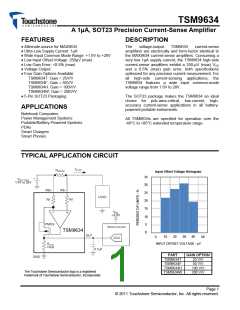
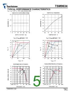
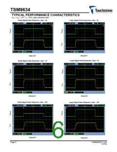
TSM9634
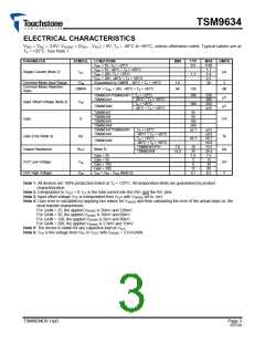
ELECTRICAL CHARACTERISTICS
VRS+ = VRS- = 3.6V; VSENSE = (VRS+ - VRS-) = 0V; TA = -40°C to +85°C, unless otherwise noted. Typical values are at
TA = +25°C. See Note 1
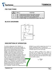
PARAMETER
SYMBOL
CONDITIONS
VRS+ = 5V, TA = +25°C
VRS+ = 5V, -40°C < TA < +85°C
VRS+ = 28V, TA = +25°C
MIN
TYP
0.5
MAX
0.85
1.1
UNITS
Supply Current (Note 2)
ICC
μA
1.1
1.8
VRS+ = 28V, -40°C < TA < +85°C
Guaranteed by CMRR , -40°C < TA < +85°C
2.5
28
Common-Mode Input Range
Common-Mode Rejection
Ratio
VCM
1.6
94
V
CMRR
1.6V < VRS+ < 28V, -40°C < TA < +85°C
130
100
dB
TA = +25°C
-40°C < TA < +85°C
TA = +25°C
250
300
250
425
TSM9634T/TSM9634F/
TSM9634H
μV
μV
Input Offset Voltage (Note 3)
VOS
100
TSM9634W
-40°C < TA < +85°C
TSM9634T
TSM9634F
25
50
Gain
G
V/V
TSM9634H
TSM9634W
TSM9634T/TSM9634F/
TSM9634H
100
200
±0.1
TA = +25°C
-40°C < TA < +85°C
TA = +25°C
-40°C < TA < +85°C
TSM9634T/F/H
TSM9634W
±0.5
±0.6
±0.7
±0.8
13.2
26.4
7.5
15
30
85
0.2
Gain Error (Note 4)
Output Resistance
GE
%
±0.1
TSM9634W
(Note 5)
7.0
14.0
10
20
1.5
3
6
12
0.1
ROUT
kΩ
Gain = 25
Gain = 50
Gain = 100
Gain = 200
OUT Low Voltage
OUT High Voltage
VOL
VOH
mV
V
VOH = VRS- - VOUT (Note 6)
Note 1: All devices are 100% production tested at TA = +25°C. All temperature limits are guaranteed by product
characterization.
Note 2: Extrapolated to VOUT = 0. ICC is the total current into the RS+ and the RS- pins.
Note 3: Input offset voltage VOS is extrapolated from VOUT with VSENSE set to 1mV.
Note 4: Gain error is calculated by applying two values for VSENSE and then calculating the error of the actual slope vs. the
ideal transfer characteristic:
For GAIN = 25, the applied VSENSE is 20mV and 120mV.
For GAIN = 50, the applied VSENSE is 10mV and 60mV.
For GAIN = 100, the applied VSENSE is 5mV and 30mV.
For GAIN = 200, the applied VSENSE is 2.5mV and 15mV.
Note 5: The device is stable for any capacitive load at VOUT
.
Note 6: VOH is the voltage from VRS- to VOUT with VSENSE = 3.6V/GAIN.
TSM9634DS r1p0
Page 3
RTFDS

 TOUCHSTONE [ TOUCHSTONE SEMICONDUCTOR INC ]