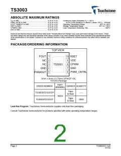
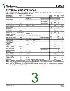
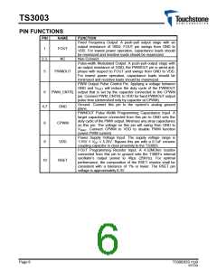
TS3003
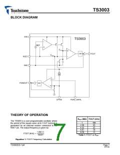
With an RSET = 4.32MΩ, the output frequency is
approximately 25kHz with a 50% duty cycle. As
design aids, Tables 1 lists TS3003’s typical ꢀOꢁT for
APPLICATIONS INFORMATION
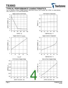
Minimizing Power Consumption
various standard values for RSET
.
To keep the TS3003’s power consumption low,
resistive loads at the FOUT and PWMOUT terminals
increase dc power consumption and therefore should
be as large as possible. Capacitive loads at the
FOUT and PWMOUT terminals increase the
TS3003’s transient power consumption and, as well,
should be as small as possible.
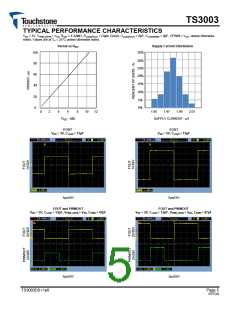
The output frequency can be user-adjusted from
10kHz to 300kHz with a single resistor. The TS3003
also provides a separate PWM output signal at its
PWMOUT terminal that is anti-phase with respect to
FOUT. A dead time of approximately 106ns exists
between FOUT and PWMOUT. To adjust the pulse
width of the PWMOUT output, a single capacitor can
be placed at the CPWM pin. To determine the
capacitance needed for a desired pulse width, the
following equation is to be used:
One challenge to minimizing the TS3003’s transient
power consumption is the probe capacitance of
oscilloscopes and frequency counter instruments.
Most instruments exhibit an input capacitance of
15pF or more. Unless buffered, the increase in
transient load current can be as much as 400nA.
ꢈulse Widthꢂsꢆ x ꢉCꢈWM
CꢈWMꢂꢀꢆ=
VCꢈWMꢀꢁꢀ300mV
Equation 2. CPWM Capacitor Calculation
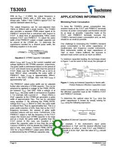
To minimize capacitive loading, the technique shown
in Figure 1 can be used. In this circuit, the principle of
where ICPWM and VCPWM is the current supplied and
voltage applied to the CPWM capacitor, respectively.
The pulse width is determined based on the period of
FOUT and should never be greater than the period at
FOUT. Make sure the PWM_CNTRL pin is set to at
least 400mV when calculating the pulse width of
PWMOUT. Note VCPWM is approximately 300mV,
which is the RSET voltage. Also note that ICPWM is
approximately 1µA.
Figure 1: Using an External Capacitor in Series with
The PWMOUT output pulse width can be adjusted
further after selecting a CPWM capacitor. This can be
achieved by applying a voltage to the PWM_CNTRL
pin between VRSET and GND. With a voltage of at
least VRSET, the pulse width is set based on Equation
Probes Reduces Effective Capacitive Load.
series-connected capacitors can be used to reduce
the effective capacitive load at the TS3003’s ꢀOꢁT
and PWMOUT terminals.
2. For example, with a period of
40µs( 25kHz) a
47pF capacitor at the CPWM pin generates a pulse
width of approximately 16µs. This can be calculated
using equation 2. By reducing the PWM_CNTRL
voltage from VRSET ꢁ 300mV to GND, the pulse width
is reduced from 16µs to approximately 8µs. This is a
pulse width reduction of 50%. Note that as the FOUT
frequency increases, the amount of pulse width
reduction reduces and vice versa. Furthermore, if the
PWMOUT output is half the frequency of the FOUT
output, this means your CPWM capacitor is too large
and as a result, the pulse width is greater than the
FOUT period. In this case, use Equation 2 and
reduce the capacitor value to less than the period.
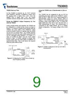
Connect CPWM to VDD to disable the PWM function
and in turn, save power. Connect PWM_CNTRL to
VDD for a fixed PWMOUT output pulse width, which
is determined by the CPWM pin capacitor only.
To determine the optimal value for CEXT once the
probe capacitance is known by simply solving for
CEXT using the following expression:
1
CꢇꢊTꢀ=ꢀ
1
ꢀ1
ꢀꢍꢀ
CꢋOAꢌꢂꢇꢀꢀꢆ CꢈROꢎꢇ
Equation 3:External Capacitor Calculation
ꢀor example, if the instrument’s input probe
capacitance is 15pF and the desired effective load
capacitance at either or both FOUT and PWMOUT
terminals is to be ≤5pꢀ, then the value of CEXT should
be ≤7.5pꢀ.
Page 8
TS3003DS r1p0
RTFDS

 TOUCHSTONE [ TOUCHSTONE SEMICONDUCTOR INC ]