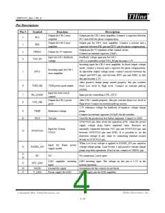
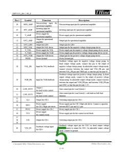
THV3543_Rev.1.00_E
Electrical Characteristics(at Vcc=12V, Ta=25℃, unless otherwise noted.)
Parameter
Whole of Circuit
Symbol
Conditions
Min
Typ
Max
Units
Average Current Consumption
Reference Voltage
Icc
VCC pin
−
5.0
−
mA
V
Vref
Cvref=0.01ꢁF
1.188
1.200
1.212
Load Regulation
Vref(load)
Iref=ꢀ100ꢁA ~ ꢀ1mA
−
−
2
2
5
8
mV
mV
(Reference Voltage)
Line Regulation
Iref=ꢀ100ꢁA
Vref(line)
(Reference Voltage)
VCC=4.2 ~ 15V
Io=ꢀ1mA
Output Voltage (5V Regulator)
Load Regulation (5V Regulator)
Vreg5(range)
Vreg5(load)
−
−
5.0
−
V
Io=ꢀ0.1mA ~ ꢀ5mA
Io=ꢀ1mA
−
100
mV
Line Regulation (5V Regulator)
Vreg5(line)
−
−
50
mV
VCC=5.5 ~ 15V
Oscillation Frequency
UVLO Release Voltage
UVLO Hysteresis Voltage
System UVLO Release Voltage
System UVLO Hysteresis
Voltage
Fosc
430
5.0
500
5.46
1.96
1.56
570
6.00
2.5
kHz
V
Vuvlo
VCC pin
Vuvlo(hys)
Vsysuvlo
VCC pin
1.4
V
SYSUVLO pin
1.44
1.68
V
Vsysuvlo(hys) SYSUVLO pin
0.41
0.56
0.71
V
CH-1 Boost Converter Block
Feedback Voltage
Vo1(fix)
15.2
15.6
Vref
−
16.0
V
V
V
V
(in fixed mode)
Feedback Voltage
Vref –
10m
Vref +
10m
Vo1(adj)
(in adjustable mode)
VO1_IN Voltage Level
(in fixed mode)
Vo1_in(fix)_th
Vo1_in(adj)_th
4.6
−
VO1_IN Voltage Level
(in adjustable mode)
Output OnꢀResistance
Output Off Leakage Current
Maximum Duty Cycle
Short Circuit Detection Threshold
Voltage
−
−
2.7
Ron(chꢀ1)
Ileak(chꢀ1)
−
−
−
100
−
170
10
−
mꢂ
ꢁA
%
Dmax(chꢀ1)
LX1 pin pulse
5
Vuvp(chꢀ1)
VO1 output voltage
−
−
−
85
−
−
−
%
ms
%
Delay Time for Short Circuit
Detection Latch
tuvp(chꢀ1)
12.2
125
Over Voltage Detection
Threshold Voltage
Vovp(chꢀ1)
VO1 output voltage
VCC=12V,
Over Current Detection
Threshold Voltage
Ics1
VO1=15.6V,
4.0
−
−
A
VO1 output current
CH-2 Buck Converter Block
Feedback Voltage
Vo2
3.23
3.30
170
3.37
290
V
Output OnꢀResistance
Ron(chꢀ2)
−
mꢂ
THine Electronics, Inc.
Copyright© 2011 THine Electronics, Inc.
8/19

 THINE [ THINE ELECTRONICS, INC. ]