L M 358N /D
FEATURES
ꢀ
ꢀ
ꢀ
ꢀ
Internally frequency compensated for unity gain
Large dc voltage gain: 100 dB
Wide bandwidth (unity gain): 1 MHz (temperature compensated)
Wide power supply range:
— Single supply: 3V to 32V
— or dual supplies: ±1.5V to ±16V
ꢀ
ꢀ
ꢀ
ꢀ
ꢀ
Very low supply current drain (500 µA)—essentially independent of supply voltage.
Low input offset voltage: 2 mV
Input common-mode voltage range includes ground
Differential input voltage range equal to the power supply voltage
Large output voltage swing: 0V to V+- 1.5V
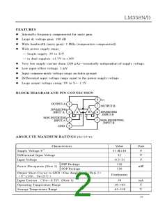
BLOCK DIAGRAM AND PIN CONNECTION
8
7
V+
OUTPUT A
1
2
OUTPUT B
INVERTING
INPUT A
B
INVERTING
INPUT B
A
-
6
5
-
+
+
NON-INVERTING
INPUT A
3
4
NON-INVERTING
INPUT B
GND
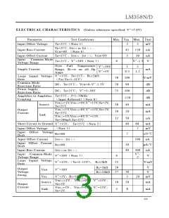
ABSOLUTE MAXIMUM RATINGS (Ta=25°C)
Characteristic
Supply Voltage,V +
Value
32 或 ±16
32
Unit
V
Differential Input Voltage
Input Voltage
V
-0.3~32
550
V
DIP Package
Power Dissipation (Note 1)
SOP Package
mW
530
Output Short-Circuit to GND( One Amplifier)( Note 2)
( V + ≤15V、 Ta=25℃ )
Continuous
Input Current ( VIN<-0.3V) (Note 3)
Operating Temperature Range
Storage Temperature Range
50
mA
℃
-20~+85
-65~150
℃
2/8

 TGS [ Tiger Electronic Co.,Ltd ]