DS_8430_001
78Q8430 Data Sheet
12 Package Mechanical Drawing (100-pin LQFP)...............................................................................86
13 Ordering Information........................................................................................................................87
14 Related Documentation....................................................................................................................87
15 Contact Information..........................................................................................................................87
Tables
Table 1: Pin Legend....................................................................................................................................12
Table 2: Clock Pin Descriptions..................................................................................................................12
Table 3: MDI Pin Descriptions.....................................................................................................................13
Table 4: LED Pin Descriptions....................................................................................................................13
Table 5: EEPROM Interface Pin Descriptions ............................................................................................13
Table 6: GBI Data Pin Descriptions ............................................................................................................14
Table 7: GBI Address Pin Descriptions.......................................................................................................15
Table 8: GBI Control Pin Descriptions ........................................................................................................15
Table 9: Chip Mode Pin Descriptions..........................................................................................................16
Table 10: JTAG Pin Descriptions................................................................................................................16
Table 11: Power Pin Descriptions...............................................................................................................17
Table 12: Absolute Maximum Ratings ........................................................................................................18
Table 13: Recommended Operating Conditions.........................................................................................18
Table 14: DC Characteristics......................................................................................................................18
Table 15: Digital I/O Characteristics ...........................................................................................................19
Table 16: MII 100Base-TX Transmit Timing ...............................................................................................19
Table 17: MII 100Base-TX Transmitter (Informative) .................................................................................19
Table 18: MII 100Base-TX Receiver Timing...............................................................................................20
Table 19: MII 10Base-T Transmitter Timing ...............................................................................................20
Table 20: MII 10Base-T Transmitter (Informative)......................................................................................20
Table 21: MII 10Base-T Receive Timing.....................................................................................................21
Table 22: Transmit Data Buffer Example....................................................................................................28
Table 23: Counter Summary.......................................................................................................................30
Table 24: CAM Rules Associated with Unicast Filter Bytes........................................................................34
Table 25: CAM Rules Associated with Multicast Filter Bytes .....................................................................36
Table 26: Control Logic Actions..................................................................................................................38
Table 27: RCR Match Control.....................................................................................................................39
Table 28: Ethernet Frame for Classification................................................................................................39
Table 29: Process Destination Address Rules............................................................................................40
Table 30: Process Source Address Rules ..................................................................................................42
Table 31: Process Length/Type, MAC Control Frames and Start IP Header Checksum Rules.................42
Table 32: Process Rules for OnNow Packet...............................................................................................43
Table 33: Process Rules for Magic Packet.................................................................................................43
Table 34: PHY Register Group ...................................................................................................................74
Table 35: Isolation Transformers ................................................................................................................83
Table 36: Reference Crystal .......................................................................................................................83
Table 37: 78Q8430 Order Numbers and Packaging Marks........................................................................87
Rev. 1.2
5

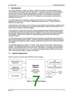
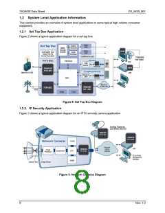
 TERIDIAN [ TERIDIAN SEMICONDUCTOR CORPORATION ]