1.5A DUAL HIGH-SPEED
POWER MOSFET DRIVERS
1
2
3
4
5
6
7
8
TC4426
TC4427
TC4428
ELECTRICAL CHARACTERISTICS (CONT.): Specifications measured over operating temperature
range with 4.5V ≤ VDD ≤ 18V, unless otherwise specified.
Symbol
Parameter
Test Conditions
Min
Typ
Max
Unit
Input
VIH
Logic 1 High Input Voltage
Logic 0 Low Input Voltage
Input Current
2.4
—
—
—
—
—
0.8
10
V
VIL
V
IIN
0V ≤ VIN ≤ VDD
– 10
µA
Output
VOH
VOL
RO
High Output Voltage
Low Output Voltage
Output Resistance
Peak Output Current
VDD – 0.025
—
—
9
—
0.025
12
V
V
Ω
A
A
—
—
VDD = 18V, IO = 10 mA
IPK
Duty Cycle ≤ 2%, t ≤ 300µsec
Duty Cycle≤ 2%
t ≤ 300µsec
—
1.5
—
—
IREV
Latch-Up Protection
> 0.5
—
Withstand Reverse Current
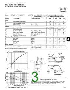
Switching Time (Note 1)
tR
Rise Time
Fall Time
Figure 1
Figure 1
Figure 1
Figure 1
—
—
—
—
—
—
—
—
40
40
40
60
nsec
nsec
nsec
nsec
tF
tD1
Delay Time
Delay Time
tD2
Power Supply
IS
Power Supply Current
VIN = 3V (Both Inputs)
VIN = 0V (Both Inputs)
—
—
—
—
8
mA
0.6
NOTE: 1. Switching times are guaranteed by design.
Crossover Energy Loss
–8
10
+5V
9
8
7
6
90%
INPUT
10%
0V
t
t
V
= 18V
DD
D1
D2
t
5
4
F
t
R
V
DD
90%
90%
4.7 µF
0.1 µF
OUTPUT
0V
6
3
10%
10%
5,7
2,4
INPUT
OUTPUT
= 1000 pF
Inverting Driver
C
L
2
+5V
90%
INPUT
–9
10
10%
3
0V
4
6
8
10
12
14
16
18
V
V
DD
90%
DD
90%
t
t
D1
D2
INPUT: 100 kHz, square wave,
= t ≤ 10ns
t
t
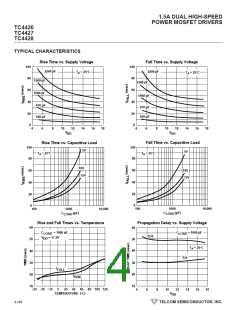
Thermal Derating Curves
F
OUTPUT
0V
R
t
RISE FALL
1600
1400
1200
1000
800
10%
10%
8 Pin DIP
Noninverting Driver
8 Pin CerDIP
8 Pin SOIC
Figure 1. Switching Time Test Circuit
600
400
200
0
NOTE: The values on this graph represent the loss seen by both drivers in a package
during one complete cycle. For a single driver, divide the stated values by 2. For a
single transition of a single driver, divide the stated value by 4.
30
40
70
80
90
100
110
120
10
20
50
60
0
AMBIENT TEMPERATURE (°C)
TELCOM SEMICONDUCTOR, INC.
4-247

 TELCOM [ TELCOM SEMICONDUCTOR, INC ]