RT6343
Operation
Control Loop
can also be synchronized with an external clock ranging
from 300kHz to 2.2MHz by RT/SYNC pin. The switching
frequency of synchronization should be equal to or higher
than the frequency set by the RT resistor. For example, if
the switching frequency of synchronization is 300kHz or
higher, the RRT/SYNC should be selected for 300kHz.
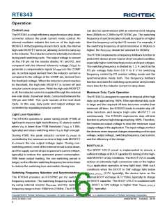
The RT6343 is a high efficiency asynchronous step-down
converter utilizes the peak current mode control. An
internal oscillator initiates the turn-on of the high-side
MOSFET.At the beginning of each clock cycle, the internal
high-side MOSFET turns on, allowing current to ramp-up
in the inductor. The inductor current is internally monitored
during each switching cycle. The output voltage is sensed
on the FB pin via the resistor divider, R1 and R2, and
compared with the internal reference voltage (VREF) to
generate a compensation signal (VCOMP) on the COMP
pin. A control signal derived from the inductor current is
compared to the voltage at the COMP pin, derived from
the feedback voltage. When the inductor current reaches
its threshold, the high-side MOSFET is turned off and
inductor current ramps down. While the high-side MOSFET
is off, the inductor current is supplied through the external
low-side diode, freewheel diode, connected between the
SW pin and GND. This cycle repeats at the next clock
cycle. In this way, duty-cycle and output voltage are
controlled by regulating inductor current.
The RT6343 implements a frequency foldback function to
protect the device at over-load or short-circuited condition,
especially higher switching frequencies and input voltages.
The switching frequency is divided by 1, 2, 4, and 8 as the
FB pin voltage falls from 0.8 V to 0 V for switching
frequency control by RT resistor setting mode and the
synchronization mode both. The frequency foldback
function increases the switching cycle period and provides
more time for the inductor current to ramp down.
Maximum Duty Cycle Operation
The RT6343 is designed to operate in dropout at the high
duty cycle approaching 100%. If the operational duty cycle
is large and the required off-time becomes smaller than
minimum off-time, the RT6343 starts to enable skip off-
time function and keeps high-side MOSFET on
continuously. The RT6343 implements skip off-time
function to achieve high duty approaching 100%. Therefore,
the maximum output voltage is near the minimum input
supply voltage of the application. The input voltage at which
the devices enter dropout changes depending on the input
voltage, output voltage, switching frequency, load current,
and the efficiency of the design.
Light Load Operation
The RT6343 operates in power saving mode (PSM) at
light load to improve light load efficiency. IC starts to switch
when VFB is lower than PSM threshold ( VREF x 1.005,
typically) and stops switching when VFB is high enough.
During PSM, the peak inductor current (IL_PEAK) is
controlled by the minimum on-time of high-side MOSFET
to ensure the low output voltage ripple. During non-
switching period, most of the internal circuit is shut down,
and the supply current drops to quiescent current (100μA,
typically) to reduce the quiescent power consumption.
With lower output loading, the non-switching period is
longer, so the effective switching frequency becomes lower
to reduce the switching loss and switch driving loss.
BOOT UVLO
The BOOT UVLO circuit is implemented to ensure a
sufficient voltage of BOOT capacitor for turning on the high-
side MOSFET at any conditions. The BOOT UVLO usually
actives at extremely high conversion ratio or the higher
VOUT application operates at very light load. With such
conditions when the BOOT to SW voltage falls below
VBOOT_UVLO_L (2.7V, typically), the device turns on the
internal BOOT recharge FET (150ns, typically) to charge
the BOOT capacitor. The BOOT UVLO is sustained until
the BOOT to SW voltage is higher than VBOOT_UVLO_H
(2.8V, typically).
Switching Frequency Selection and Synchronization
The RT6343 provides an RT/SYNC pin for switching
frequency selection. The switching frequency can be set
by using external resistor RRT/SYNC and the switching
frequency range is from 100kHz to 2.5MHz. The RT6343
Copyright 2019 Richtek Technology Corporation. All rights reserved.
©
is a registered trademark of Richtek Technology Corporation.
www.richtek.com
6
DS6343-00 October 2019

 RICHTEK [ RICHTEK TECHNOLOGY CORPORATION ]