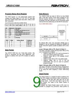
VRS51C1000
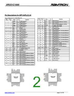
Pin Descriptions for QFP-44/PLCC-44
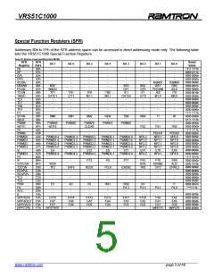
TABLE 1: PIN DESCRIPTIONS FOR QFP-44/PLCC-44
QFP
- 44
PLCC
- 44
Name
P2.6
I/O
I/O
Function
QFP
- 44
PLCC
- 44
Name
I/O
Function
PWM Channel 2
Bit 5 of Port 1
PWM Channel 3
Bit 6 of Port 1
PWM Channel 4
Bit 7 of Port 1
Reset
Receive Data
Bit 0 of Port 3
Bit 3 of Port 4
Transmit Data &
Bit 1 of Port 3
External Interrupt 0
Bit 2 of Port 3
External Interrupt 1
Bit 3 of Port 3
Timer 0
Bit 4 of Port 3
Timer 1 & 3
Bit 5 of Port
Ext. Memory Write
Bit 6 of Port 3
Ext. Memory Read
Bit 7 of Port 3
Oscillator/Crystal Output
Oscillator/Crystal In
Ground
Bit 0 of Port 4
Bit 0 of Port 2
Bit 8 of External Memory Address
Bit 1 of Port 2
Bit 6 of Port 2
24
25
30
31
PWM2
P1.5
PWM3
P1.6
PWM4
P1.7
RES
RXD
P3.0
P4.3
TXD
P3.1
#INT0
P3.2
#INT1
P3.3
T0
O
I/O
O
I/O
O
I/O
I
1
2
7
8
A14
P2.7
A15
O
I/O
O
O
O
Bit 14 of External Memory Address
Bit 7 of Port 2
Bit 15 of External Memory Address
Program Store Enable
Address Latch Enable
Bit 1 of Port 4
External Access
Bit 7 Of Port 0
Data/Address Bit 7 of External Memory
Bit 6 of Port 0
Data/Address Bit 6 of External Memory
Bit 5 of Port 0
Data/Address Bit 5 of External Memory
Bit 4 of Port 0
Data/Address Bit 4 of External Memory
Bit 3 Of Port 0
Data/Address Bit 3 of External Memory
Bit 2 of Port 0
Data/Address Bit 2 of External Memory
Bit 1 of Port 0 & Data
Address Bit 1 of External Memory
Bit 0 Of Port 0 & Data
Address Bit 0 of External Memory
VCC
26
27
28
29
32
33
34
35
#PSEN
ALE
P4.1
#EA
P0.7
AD7
P0.6
AD6
P0.5
AD5
P0.4
AD4
P0.3
AD3
P0.2
AD2
P0. 1
AD1
P0.0
AD0
VDD
P4.2
T2
3
4
5
6
7
9
I/O
I
10
11
12
13
I
I/O
I/O
I/O
I/O
I/O
I/O
I/O
I/O
I/O
I/O
I/O
I/O
I/O
I/O
I/O
I/O
-
30
31
32
33
34
35
36
37
36
37
38
39
40
41
42
43
I/O
I/O
O
I/O
I
I/O
I
I/O
I
I/O
I
I/O
O
I/O
O
I/O
O
8
14
15
16
17
18
19
9
10
11
12
13
P3.4
T1
P3.5
#WR
P3.6
#RD
P3.7
XTAL2
XTAL1
VSS
P4.0
P2.0
A8
38
39
44
1
14
15
16
17
20
21
22
23
I/O
I
Bit 2 of Port 4
Timer 2 Clock Out
I
-
I/O
I/O
O
40
2
P1.0
T2EX
P1.1
P1.2
I/O
I
I/O
I/O
Bit 0 of Port 1
Timer 2 Control
Bit 1 of Port 1
Bit 2 of Port 1
41
42
3
4
18
19
20
21
24
25
26
27
28
29
P2.1
A9
P2.2
A10
P2.3
A11
P2.4
A12
I/O
O
I/O
O
I/O
O
I/O
O
PWM0
P1.3
O
PWM Channel 0
Bit 3 of Port 1
Bit 9 of External Memory Address
Bit 2 of Port 2
Bit 10 of External Memory Address
Bit 3 of Port 2 &
Bit 11 of External Memory Address
Bit 4 of Port 2
Bit 12 of External Memory Address
Bit 5 of Port 2
43
44
5
6
I/O
O
PWM1
P1.4
PWM Channel 1
Bit 4 of Port 1
I/O
22
23
P2.5
A13
I/O
O
Bit 13 of External Memory Address
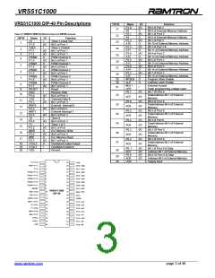
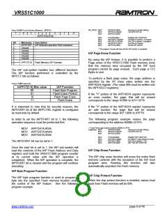
6
5
1
44 43 42 41 40
4
3
2
6
5
1
44 43 42 41 40
4
3
2
7
8
9
39
PWM2/P1.5
P0.4/AD4
7
8
9
39
PWM2/P1.5
P0.4/AD4
P0.5/AD5
P0.6/AD6
38
PWM3/P1.6
PWM4/P1.7
RES
P0.5/AD5
P0.6/AD6
P0.7/AD7
#EA
38
PWM3/P1.6
PWM4/P1.7
RES
37
36
35
34
33
32
37
36
35
34
33
10
11
P0.7/AD7
#EA
10
11
RXD/P3.0
P4.3
VRS51C1000
PLCC-44
RXD/P3.0
P4.3
VRS51C1000
PLCC-44
12
13
P4.1
12
13
P4.1
TXD/P3.1
#INT0/P3.2
#INT1/P3.3
T0/P3.4
ALE
TXD/P3.1
#INT0/P3.2
#INT1/P3.3
T0/P3.4
ALE
14
15
16
17
#PSEN
P2.7/A15
P2.6/A14
P2.5/A13
32
31
30
29
14
15
16
17
#PSEN
P2.7/A15
P2.6/A14
P2.5/A13
31
30
29
T1/P3.5
T1/P3.5
28
18 19 20 21 22 23 24 25 26 27
28
18 19 20 21 22 23 24 25 26 27
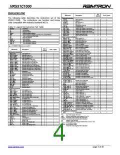
______________________________________________________________________________________________
www.ramtron.com page 2 of 48

 RAMTRON [ RAMTRON INTERNATIONAL CORPORATION ]