VRS51C1000
Program Status Word Register
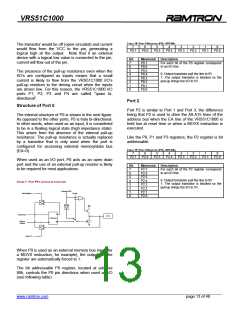
Data Memory
The VRS51C1000 has total of 1KB of on-chip SRAM
with a 256 byte subset of this block mapped as the
internal memory structure of a standard 8052. The
remaining 768 byte sub-block can be accessed using
external memory addressing via the MOVX instruction.
The PSW register is a bit addressable register that
contains the status flags (CY, AC, OV, P), user flag
(F0) and register bank select bits (RS1, RS0) of the
8051 processor.
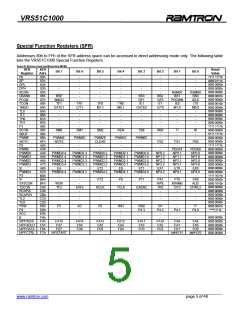
TABLE 12: PROGRAM STATUS WORD REGISTER (PSW) - SFR DOH
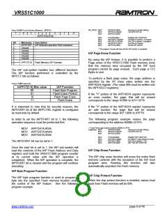
FIGURE 5: VRS51C1000 DATA MEMORY
7
CY
6
AC
5
F0
4
RS1
3
RS0
2
OV
1
-
0
P
02FF
Bit
Mnemonic Description
7
6
5
4
3
2
1
0
CY
AC
F0
RS1
RS0
OV
-
Carry Bit
Auxiliary Carry Bit from bit 3 to 4.
User definer flag
R0-R7 Registers bank select bit 0
R0-R7 Registers bank select bit 1
Overflow flag
Expanded 768 bytes
(accessed by direct
external addressing mode,
using the MOVX
instruction)
(XRAME=1)
FF
Upper 128 bytes
(Indirect addressing mode only)
SFR
-
(Direct addressing mode only)
80
7F
P
Parity flag
Lower 128 bytes
00
0000
RS1
RS0
Active Bank
Address
0
0
1
1
0
1
0
1
0
1
2
3
00h-07h
08h-0Fh
10h-17h
18-1Fh
By default after reset, the expanded SRAM area is
disabled. It can be enabled by setting the XRAME bit
of the SYSCON register located at address BFh in the
SFR.
Lower 128 bytes (00h to 7Fh, Bank 0 & Bank 1)
The lower 128 bytes of data memory (from 00h to 7Fh)
can is summarized as follows:
Data Pointer
The VRS51C1000 has one 16-bit data pointer. The
DPTR is accessed via two SFR addresses: DPL
located at address 82h and DPH located at address
83h.
o
Address range 00h to 7Fh can be accessed in
direct and indirect addressing modes.
Address range 00h to 1Fh includes R0-R7
registers area.
o
o
o
Address range 20h to 2Fh is bit addressable.
Address range 30h to 7Fh is not bit
addressable and can be used as general-
purpose storage.
Upper 128 bytes (80h to FFh, Bank 2 & Bank 3)
The upper 128 bytes of the data memory ranging from
80h to FFh can be accessed using indirect addressing
or by using the bank mapping in direct addressing
mode.
Stack Pointer
The Stack Pointer is a register located at address 81h
of the SFR register area whose value corresponds to
the address of the last item that was put on the
processor stack. Each time new data is put on the
Stack Pointer, the value of the Stack Pointer is
incremented.
By default, the Stack Pointer value is 07h, but it is
possible to program the processor stack pointer to
______________________________________________________________________________________________
www.ramtron.com page 9 of 48

 RAMTRON [ RAMTRON INTERNATIONAL CORPORATION ]