FM25L16B - 16Kb 3V SPI F-RAM
The BP1 and BP0 bits and the Write Enable Latch
are the only mechanisms that protect the memory
from writes. The remaining write protection features
protect inadvertent changes to the block protect bits.
This scheme provides a write protection mechanism,
which can prevent software from writing the
memory under any circumstances. This occurs if the
BP1 and BP0 are set to 1, the WPEN bit is set to 1,
and /WP is set to 0. This occurs because the block
protect bits prevent writing memory and the /WP
signal in hardware prevents altering the block
protect bits (if WPEN is high). Therefore in this
condition, hardware must be involved in allowing a
write operation. The following table summarizes the
write protection conditions.
The WPEN bit controls the effect of the hardware
/WP pin. When WPEN is low, the /WP pin is
ignored. When WPEN is high, the /WP pin controls
write access to the status register. Thus the Status
Register is write protected if WPEN=1 and /WP=0.
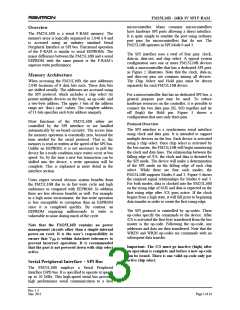
Table 4. Write Protection
WEL
WPEN
/WP
X
X
0
1
Protected Blocks
Protected
Protected
Protected
Protected
Unprotected Blocks
Protected
Unprotected
Unprotected
Unprotected
Status Register
Protected
Unprotected
Protected
0
1
1
1
X
0
1
1
Unprotected
8th clock). The rising edge of /CS terminates a
WRITE op-code operation.
Memory Operation
The SPI interface, which is capable of a relatively
high clock frequency, highlights the fast write
capability of the F-RAM technology. Unlike SPI-bus
EEPROMs, the FM25L16B can perform sequential
writes at bus speed. No page register is needed and
any number of sequential writes may be performed.
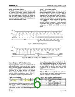
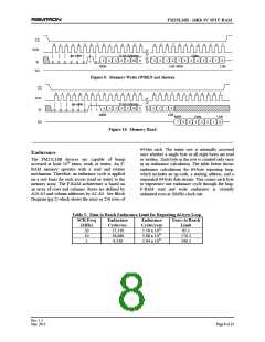
Read Operation
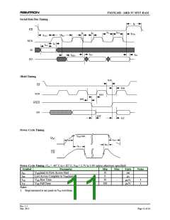
After the falling edge of /CS, the bus master can issue
a READ op-code. Following this instruction is a two-
byte address value. The upper 5-bits of the address
are ignored. In total, the 11-bits specify the address of
the first byte of the read operation. After the op-code
and address are complete, the SI line is ignored. The
bus master issues 8 clocks, with one bit read out for
each. Addresses are incremented internally as long as
the bus master continues to issue clocks. If the last
address of 7FFh is reached, the counter will roll over
to 000h. Data is read MSB first. The rising edge of
/CS terminates a READ op-code operation. A read
operation is shown in Figure 10.
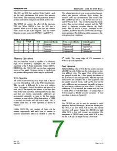
Write Operation
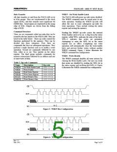
All writes to the memory array begin with a WREN
op-code. The next op-code is the WRITE instruction.
This op-code is followed by a two-byte address
value. The upper 5-bits of the address are ignored. In
total, the 11-bits specify the address of the first data
byte of the write operation. Subsequent bytes are data
and they are written sequentially. Addresses are
incremented internally as long as the bus master
continues to issue clocks. If the last address of 7FFh
is reached, the counter will roll over to 000h. Data is
written MSB first. A write operation is shown in
Figure 9.
Hold
The /HOLD pin can be used to interrupt a serial
operation without aborting it. If the bus master pulls
the /HOLD pin low while SCK is low, the current
operation will pause. Taking the /HOLD pin high
while SCK is low will resume an operation. The
transitions of /HOLD must occur while SCK is low,
but the SCK pin can toggle during a hold state.
Unlike EEPROMs, any number of bytes can be
written sequentially and each byte is written to
memory immediately after it is clocked in (after the
Rev. 1.3
Mar. 2011
Page 7 of 14

 RAMTRON [ RAMTRON INTERNATIONAL CORPORATION ]