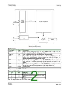
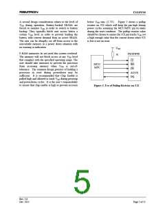
FM18W08
/CE goes inactive. Data becomes available on the bus
after the access time has been satisfied.
Overview
The FM18W08 is a bytewide F-RAM memory. The
memory array is logically organized as 32,768 x 8
and is accessed using an industry standard parallel
interface. All data written to the part is immediately
nonvolatile with no delay. Functional operation of the
F-RAM memory is the same as SRAM type devices,
except the FM18W08 requires a falling edge of /CE
to start each memory cycle.
After the address has been latched, the address value
may be changed upon satisfying the hold time
parameter. Unlike an SRAM, changing address values
will have no effect on the memory operation after the
address is latched.
The FM18W08 will drive the data bus when /OE is
asserted low. If /OE is asserted after the memory
access time has been satisfied, the data bus will be
driven with valid data. If /OE is asserted prior to
completion of the memory access, the data bus will
not be driven until valid data is available. This feature
minimizes supply current in the system by eliminating
transients caused by invalid data being driven onto
the bus. When /OE is inactive the data bus will
remain tri-stated.
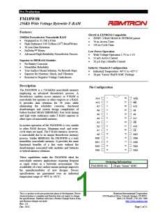
Memory Architecture
Users access 32,768 memory locations each with 8
data bits through a parallel interface. The complete
15-bit address specifies each of the 32,768 bytes
uniquely. Internally, the memory array is organized
into 4092 rows of 8-bytes each. This block
segmentation has no effect on operation, however the
user may wish to group data into blocks by its
endurance characteristics as explained on page 4.
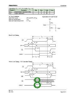
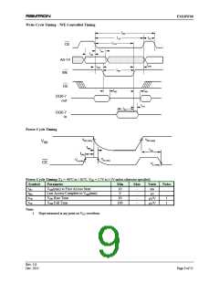
Write Operation
Writes occur in the FM18W08 in the same time
interval as reads. The FM18W08 supports both /CE-
and /WE-controlled write cycles. In all cases, the
address is latched on the falling edge of /CE.
The cycle time is the same for read and write memory
operations. This simplifies memory controller logic
and timing circuits. Likewise the access time is the
same for read and write memory operations. When
/CE is deasserted high, a precharge operation begins,
and is required of every memory cycle. Thus unlike
SRAM, the access and cycle times are not equal.
Writes occur immediately at the end of the access
with no delay. Unlike an EEPROM, it is not
necessary to poll the device for a ready condition
since writes occur at bus speed.
In a /CE controlled write, the /WE signal is asserted
prior to beginning the memory cycle. That is, /WE is
low when /CE falls. In this case, the part begins the
memory cycle as a write. The FM18W08 will not
drive the data bus regardless of the state of /OE.
In a /WE controlled write, the memory cycle begins
on the falling edge of /CE. The /WE signal falls after
the falling edge of /CE. Therefore, the memory cycle
begins as a read. The data bus will be driven
according to the state of /OE until /WE falls. The
timing of both /CE- and /WE-controlled write cycles
is shown in the electrical specifications.
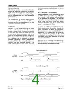
It is the user’s responsibility to ensure that VDD
remains within datasheet tolerances to prevent
incorrect operation. Also proper voltage level and
timing relationships between VDD and /CE must be
maintained during power-up and power-down events.
See Power Cycle Timing diagram on page 9.
Write access to the array begins asynchronously after
the memory cycle is initiated. The write access
terminates on the rising edge of /WE or /CE,
whichever is first. Data set-up time, as shown in the
electrical specifications, indicates the interval during
which data cannot change prior to the end of the write
access.
Memory Operation
The FM18W08 is designed to operate in a manner
similar to other bytewide memory products. For users
familiar with BBSRAM, the performance is
comparable but the bytewide interface operates in a
slightly different manner as described below. For
users familiar with EEPROM, the obvious differences
result from the higher write performance of F-RAM
technology including NoDelay writes and much
higher write endurance.
Unlike other truly nonvolatile memory technologies,
there is no write delay with F-RAM. Since the read
and write access times of the underlying memory are
the same, the user experiences no delay through the
bus. The entire memory operation occurs in a single
bus cycle. Therefore, any operation including read or
write can occur immediately following a write. Data
Read Operation
A read operation begins on the falling edge of /CE.
At this time, the address bits are latched and a
memory cycle is initiated. Once started, a full
memory cycle must be completed internally even if
polling,
a technique used with EEPROMs to
determine if a write is complete, is unnecessary.
Rev. 2.0
Dec. 2011
Page 3 of 11

 RAMTRON [ RAMTRON INTERNATIONAL CORPORATION ]