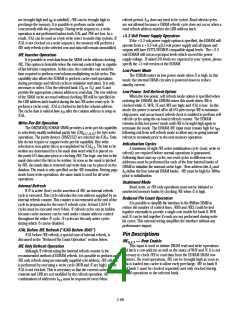
/CAL0-3,P — Column Address Latch
This input is used to latch the column address and in
combination with /WE to trigger write operations. When /CAL is
/S0,1 — Chip Select
This input is used to power up the I/O and clock circuitry.
When /S is high, the EDRAM remains in its low power mode. /S
high, the column address latch is transparent. When /CAL is low, the must be used for bank selection on the 8Mbyte SIMM. /S must
column address is closed and the output of the latch contains the remain active throughout any read or write operation. With the
address present while /CAL was high. It also controls the operation exception of /F refresh cycles, /RE should never be clocked when /S
of the output data latch. Data is latched while /CAL is high and the
latch is transparent when /CAL is low.
is inactive.
DQ0-35 — Data Input/Output
W/R — Write/Read
These bidirectional data pins are used to read and write data to
the EDRAM. On the DM2252 write-per-bit memory, these pins are
also used to specify the bit mask used during write operations.
This input along with /F specifies the type of DRAM operation
initiated on the low going edge of /RE. When /F is high, W/R
specifies either a write (logic high) or read operation (logic low).
A0-10 — Multiplex Address
/F — Refresh
These inputs are used to specify the row and column addresses
of the EDRAM data. The 11-bit row address is latched on the falling
This input will initiate a DRAM refresh operation using the
internal refresh counter as an address source when it is low on the edge of /RE. The 9-bit column address can be specified at any other
low going edge of /RE.
time to select read data from the SRAM cache or to specify the write
column address during write cycles.
/WE — Write Enable
This input controls the latching of write data on the input data V Power Supply
pins. A write operation is initiated when both /CAL and /WE are low.
CC These inputs are connected to the +5 or 3.3 volt power supply.
V Ground
/G — Output Enable
SS
These inputs are connected to the power supply ground
connection.
This input controls the gating of read data to the output data
pin during read operations.
Capacitance
Absolute Maximum Ratings
(Beyond Which Permanent Damage Could Result)
Description
Max*
130/136pf
165/180pf
97/100pf
52pf
Pins
3.3V Option
Description
Input Voltage (V )
Ratings
- 1 ~ 7v
- 1 ~ 7v
- 1 ~ 7v
Rating
Input Capacitance
Input Capacitance
Input Capacitance
Input Capacitance
Input Capacitance
Input Capacitance
Input Capacitance
Input Capacitance
Input Capacitance
I/O Capacitance
A
0-10
- .5 ~ 4.6v
IN
W/R, /WE, /F
/S , /S
Output Voltage (VOUT
)
- .5 ~ 4.6v
- .5 ~ 4.6v
0
1
Power Supply Voltage (V )
CC
/RE
0
Ambient Operating Temperature (TA) -40 ~ +85°C -40 ~ +85°C
55/65pf
92/96pf
62/64pf
52/55pf
32pf
/RE
2
Storage Temperature (TS)
-55 ~ 150°C -55 ~ 150°C
/RE
3
Static Discharge Voltage
(Per MIL-STD-883 Method 3015)
Class 1
20mA*
Class 1
50mA*
/G
Short Circuit O/P Current (IOUT
)
/CAL
0-3
* One output at a time per device; short duration
/CAL
P
DQ
16pf
0-35
* DM2M32SJ6/DM2M36SJ6, respectively
2-102

 RAMTRON [ RAMTRON INTERNATIONAL CORPORATION ]