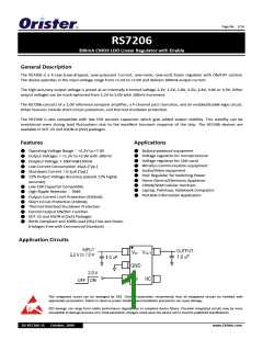
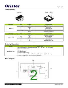
Page No. : 5/16
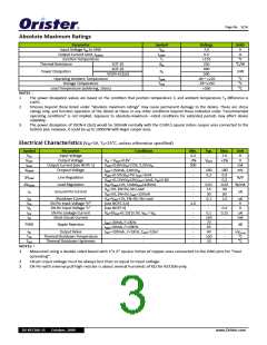
(TJ −TA)
θJC + θCA
(TJ −TA)
PMAX =
=
θJA
Where (TJ‐TA) is the temperature difference between the RS7206 die junction and the surrounding air, θJC is the thermal
resistance of the package chosen, and θCA is the thermal resistance through the printed circuit board, copper traces and
other materials to the surrounding air. For better heat‐sinking, the copper area should be equally shared between the VIN,
VOUT, and GND pins.
The thermal resistance θJA of SOT‐25 package of RS7206 is 250°C/W. Based on a maximum operating junction temperature
125°C with an ambient of 25°C, the maximum power dissipation will be:
(TJ −TA)
θJC + θCA
(125 − 25 )
PMAX =
=
= 0.40W
250
Thermal characteristics were measured using a double sided board with 1”x2” square inches of copper area connected to the
GND pin for “heat spreading”.
Dropout Voltage
A regulator’s minimum input‐output voltage differential, or dropout voltage, determines the lowest usable supply voltage. In
battery‐powered systems, this will determine the useful end‐of‐life battery voltage. The RS7206 use a P‐ channel MOSFET
pass transistor, its dropout voltage is a function of drain‐to‐source on‐resistance RDS(ON) multiplied by the load current.
VDROPOUT =VIN −VOUT = RDS (ON ) × IOUT
DS‐RS7206‐15 October, 2009
www.Orister.com

 ORISTER [ ORISTER CORPORATION ]