Page No. : 2/16
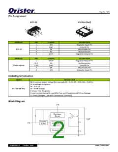
Pin Assignment
SOT‐25
VSON‐6 (2x2)
PACKAGE
PIN
1
2
3
4
SYMBOL
VIN
GND
EN
DESCRIPTION
Regulator Input Pin
Ground Pin
Chip Enable Pin
No Connection
SOT‐25
NC
5
VOUT
Regulator Output Pin
PACKAGE
PIN
1
2, 5
3, EP
4
SYMBOL
VOUT
NC
GND
EN
DESCRIPTION
Regulator Output Pin
No Connection
Ground Pin
Chip Enable Pin
Regulator Input Pin
VSON‐6 (2x2)
6
VIN
Ordering Information
DEVICE
DEVICE CODE
XX is nominal output voltage (for example, 15 = 1.5V, 33 = 3.3V, 285 = 2.85V).
YY is package designator :
NE : SOT‐25
RS7206‐XX YY Z
VF : VSON‐6 (2x2)
Z is Lead Free designator :
P: Commercial Standard, Lead (Pb) Free and Phosphorous (P) Free Package
G: Green (Halogen Free with Commercial Standard)
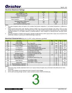
Block Diagram
DS‐RS7206‐15 October, 2009
www.Orister.com

 ORISTER [ ORISTER CORPORATION ]