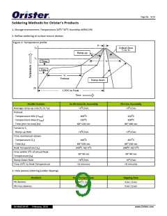
Page No. : 2/10
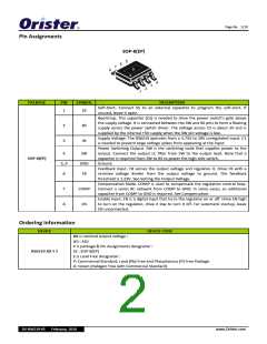
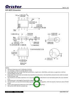
Pin Assignments
SOP‐8(EP)
PACKAGE
PIN
SYMBOL
DESCRIPTION
Soft‐Start. Connect SS to an external capacitor to program the soft‐start. If
unused, leave it open.
1
2
3
SS
Bootstrap. This capacitor (C5) is needed to drive the power switch’s gate above
the supply voltage. It is connected between the SW and BS pins to form a floating
supply across the power switch driver. The voltage across C5 is about 5V and is
supplied by the internal +5V supply when the SW pin voltage is low.
Supply Voltage. The RS6519 operates from a 4.75V to 20V unregulated input. C1
is needed to prevent large voltage spikes from appearing at the input.
Power Switching Output. SW is the switching node that supplies power to the
output. Connect the output LC filter from SW to the output load. Note that a
capacitor is required from SW to BS to power the high‐side switch.
Ground.
BS
IN
4
5, 9
6
SW
GND
FB
SOP‐8(EP)
Feedback Input. FB senses the output voltage and regulates it. Drive FB with a
resistive voltage divider from the output voltage to ground. The feedback
threshold is 1.23V. See Setting the Output Voltage.
Compensation Node. COMP is used to compensate the regulation control loop.
Connect a series RC network from COMP to GND. In some cases, an additional
capacitor from COMP to GND is required. See Compensation.
Enable Input. EN is a digital input that turns the regulator on or off. Drive EN high
to turn on the regulator, drive it low to turn it off. For automatic startup, leave
EN unconnected.
7
8
COMP
EN
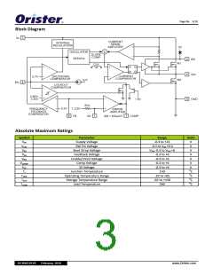
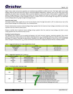
Ordering Information
DEVICE
DEVICE CODE
XX is nominal output voltage :
AD : ADJ
Y is package & Pin Assignments designator :
SE : SOP‐8(EP)
RS6519‐XX Y Z
Z is Lead Free designator :
P: Commercial Standard, Lead (Pb) Free and Phosphorous (P) Free Package
G: Green (Halogen Free with Commercial Standard)
DS‐RS6519‐05 February, 2010
www.Orister.com

 ORISTER [ ORISTER CORPORATION ]