Page No. : 3/3
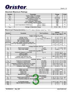
Absolute Maximum Ratings
Symbol
Parameter
Range
Units
VDD
VFB
VSense
PD
Supply voltage Pin Voltage
Input Voltage to FB Pin
Input Voltage to SENSE Pin
Power Dissipation
ESD Capability, HBM Model
ESD Capability, Machine Model
40
-0.3 to 6V
-0.3 to 6V
1000
V
V
V
mW
V
V
2000
200
DIP-8(10sec)
SOP-8(10sec)
Storage Temperature Range
260
230
TL
Lead Temperature (Soldering)
oC
oC
TSTG
-55 to + 150
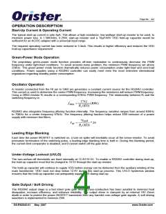
Electrical Characteristics (Ta=27°C unless otherwise noted, VDD = 15V.)
RS2042
Symbol
Parameter
Test Conditions
Unit
Min Typ Max
Supply Voltage (VDD Pin)
IST
ISS
Startup Current
Operating Current
Start Threshold Voltage
VDD=17
VFB= VSENSE = 0V VDD=15
7.5
3.0
30
5
μA
mA
V
V
V
VTH (ON)
VTH (OFF)
VDD-OVP
--
--
16.0 16.5 17.0
10.4 10.8 11.2
23.0 24.5 25.0
Min. Operating Voltage
VDD Over Voltage Protection (Latch off)
VDD Low-Threshold Voltage to Exit Green-OFF
Mode
VDD-th-g
11.0 12.0 13.0
V
Voltage Feedback (FB Pin)
IFB
VFB
Short Circuit Current
Open Loop Voltage
VFB=0V
VFB=Open
1.42
6.00
mA
V
Current Sensing (SEN Pin)
VTH
TPD
ZCS
Threshold voltage for current limit
Delay to Output
IVIN =0
0.76 0.9
115 200
13
V
nsec
KΩ
Input Impedance
260 354 460
nsec
Bnk
Leading Edge Blanking Time
VTH
Threshold voltage for current limit
IVIN =0
0.76 0.9
V
Oscillator (RI Pin)
FOSC
FOSC-green
VN
Frequency in nominal mode
Frequency in green mode
Beginning of frequency reducing at FB Voltage
End of frequency reducing at FB voltage
Frequency Temp. Stability
RI=26KΩ
RI=26 KΩ
VDD=15V
VDD=15V
-30-85oC
63
25
67
27
70
29
KHz
KHz
V
VG
%
1.95 2.05 2.15
1.50 1.54 1.60
5.0
VG
GATE Drive Output (GATE Pin)
VOL
VOH
TR
TF
DCMAX
Output Low Level
Output High Level
Rising Time
Falling Time
Maximum Duty Cycle
VDD=12V, IO=50mA
VDD=12V, IO=50mA
VDD=15V,CL=1nF
VDD=13V,CL=1nF
0.32 0.60
7.2 8.00
200 240 280
V
V
ns
ns
30
84
80
86
90
88
Over-Temperature Protection Section
IRT
Output current of pin RT
RI=26KΩ
65
70
75
μA
VOTP
Threshold voltage for over-temperature protection.
1.00 1.05 1.10
V
RI Section
RINOR
RIMAX
RIMIN
RI Operating Range
Max RI value for Protection
15.5
26
216
6
36
KΩ
KΩ
KΩ
DS-RS2042-01 May, 2007
www.Orister.com

 ORISTER [ ORISTER CORPORATION ]