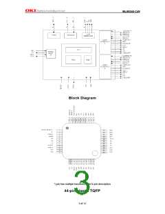
ML69240-C49
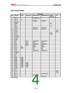
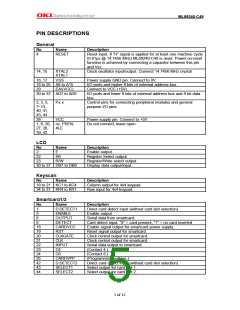
PIN DESCRIPTIONS
General
No
Name
Description
4
RESET
Reset input. If “H” signal is applied for at least one machine cycle
(0.81µs @ 14.7456 MHz) ML69240-C49 is reset. Power-on-reset
function is achieved by connecting a capacitor between this pin
and Vcc.
14, 15
16, 17
18 to 25 A8 to A15
29 EA/(VCC)
30 to 37 AD7 to AD0
XTAL2
XTAL1
VSS
Clock oscillator input/output. Connect 14.7456 MHz crystal.
Power supply GND pin. Connect to 0V.
I/O ports and higher 8 bits of external address bus.
Connect to VCC (+5V).
I/O ports and lower 8 bits of external address bus and 8 bit data
bus.
2, 3, 5,
7~13,
Px.x
Control pins for connecting peripheral modules and general
purpose I/O pins.
40, 41,
43, 44
38
VCC
Power supply pin. Connect to +5V
Do not connect, leave open.
1, 6, 26, nc, PSEN,
27, 28,
ALE
39, 42
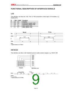
LCD
No
2
Name
E
Description
Enable output.
22
23
RS
R/W
Register Select output.
Register/Write select output.
Display data output/input.
30 to 37 DB7 to DB0
Keyscan
No
Name
Description
18 to 21 KC1 to KC4
34 to 37 KR4 to KR1
Column output for 4x4 keypad.
Row input for 4x4 keypad.
Smartcard1/2
No
Name
Description
1
3
8
9
D.DETECT1
ENABLE
OUTPUT
DETECT
CARDVCC
RST
CLKGATE
CLK
INPUT
Direct card detect input (without card slot selection)
Enable output.
Serial data from smartcard.
Card detect input. “0” = card present, “1” = no card inserted
Enable signal output for smartcard power supply.
Reset signal output for smartcard.
Clock control output for smartcard.
Clock control output for smartcard.
Serial data output to smartcard.
(Contact 4.)
(Contact 8.)
(Programming voltage.)
Direct card detect input (without card slot selection)
Select output for card slot 1.
Select output for card slot 2.
18
19
20
21
22
23
24
25
42
43
44
C4
C8
CARDVPP
D.DETECT2
SELECT1
SELECT2
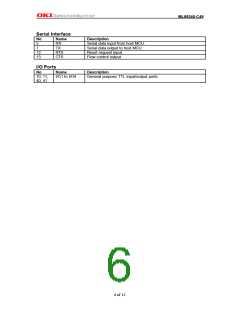
5 of 13

 OKI [ OKI ELECTRONIC COMPONETS ]