FEDL66517-01
1
Semiconductor
ML66517 Family
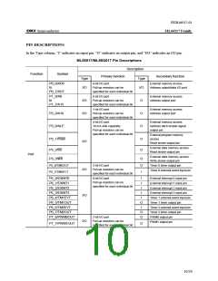
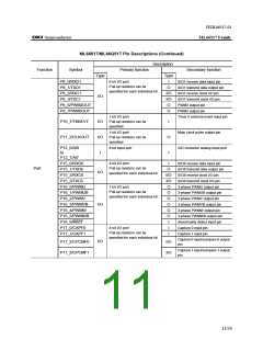
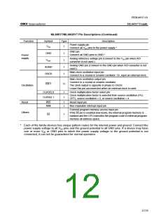
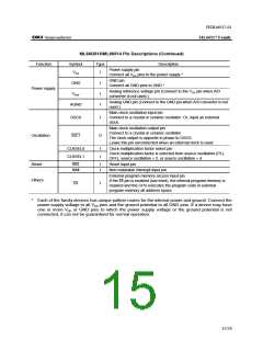
ML66517/ML66Q517 Pin Descriptions (Continued)
Function
Symbol
Type
I
Description
Power supply pin
VDD
GND
VREF
Connect all VDD pins to the power supply.*
GND pin
I
I
I
I
Connect all GND pins to GND.*
Power
supply
Analog reference voltage pin (Connect to the VDD pin when A/D
converter is not used.)
Analog GND pin (Connect to the GND pin when A/D converter is not
used.)
AGND
OSC0
Main clock oscillation input pin
Connect to a crystal or ceramic oscillator. Or, input an external clock.
Main clock oscillation output pin
Connect to a crystal or ceramic oscillator.
The clock output is opposite in phase to OSC0.
Leave this pin unconnected when an external clock is used.
OSC1
O
Oscillation
CLKSEL0
CLKSEL1
I
I
Clock multiplication factor select pin
Clock multiplication factor is selected from source oscillation (PLL
OFF), source oscillation × 2, or source oscillation × 4
Reset
RES
NMI
I
I
Reset input pin
Non-maskable interrupt input pin
External program memory access input pin
Others
If the EA pin is enabled (low level), the internal program memory is
masked and the CPU executes the program code in external program
memory all address space.
EA
I
*
Each of the family devices has unique pattern routes for the internal power and ground. Connect the
power supply voltage to all VDD pins and the ground potential to all GND pins. If a device may have
one or more VDD or GND pins to which the power supply voltage or the ground potential is not
connected, it can not be guaranteed for normal operation.
12/29

 OKI [ OKI ELECTRONIC COMPONETS ]