FEDL2250DIGEST-01
OKI Semiconductor
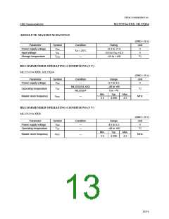
ML2252/54-XXX, ML22Q54
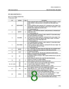
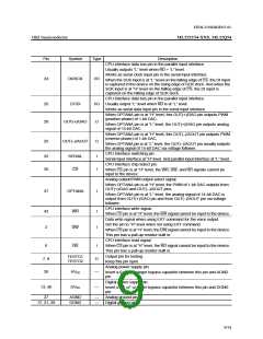
Pin
24
Symbol
D6/SCK
Type
I/O
Description
CPU interface data bus pin in the parallel input interface.
Usually outputs “L” level when RD = “L” level.
Works as serial clock input pin in the serial input interface.
When the SCK input is at “L” level on the falling edge of CS, the DI input
is captured in the device on the rising edge of SCK clock. And when the
SCK input is at “H” level on the falling edge of CS, the DI input is
captured on the falling edge of SCK clock.
CPU interface data bus pin in the parallel input interface.
Usually output “L” level when RD is at “L” level.
26
D7/DI
I/O
O
Works as serial data input pin in the serial input interface.
When OPTANA pin is at “H” level, this OUT(+)/DAO pin outputs PWM
(positive phase) of 1-bit DAC.
28
29
OUT(+)/DAO
OUT(–)/AOUT
When OPTANA pin is at “L” level, the OUT(+)/DAO pin outputs analog
signal of 14-bit DAC.
When OPTANA pin is at “H” level, this OUT(–)/AOUT pin outputs PWM
(reverse phase) of 1-bit DAC.
O
When OPTANA pin is at “L” level, the OUT(–)/AOUT pin usually outputs
the analog signal of 14-bit DAC via voltage follower.
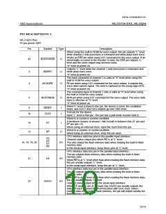
CPU interface switching pin.
32
36
SERIAL
I
I
Serial input interface at “H” level. And parallel input interface at “L” level.
CPU interface chip select pin.
CS
When CS pin is at “H” level, the WR, DW, and RD signals cannot be
input to the device.
Analog output/PWM output select signal.
When OPTANA pin is at “H” level, the PWM of 1-bit DAC outputs from
OUT(+)/DAO and OUT(–)/AOUT pins.
37
OPTANA
I
When OPTANA pin is at “L” level, the analog signal of 14-bit DAC is
output from OUT(+)/DAO pin and from OUT(–)/AOUT pin via voltage
follower.
CPU interface write signal.
42
2
WR
DW
I
I
When CS pin is at “H” level, the WR signal cannot be input to the device.
Data write signal when using EXT command for the voice output.
Set the pin to “H” level when not using EXT command.
When CS pin is at “H” level, the DW signal cannot be input to the device.
This pin has a pull-up resistor built in.
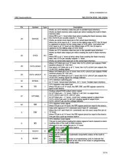
CPU interface read signal.
6
RD
I
When CS pin is at “H” level, the RD signal cannot be input to the device.
This pin has a pull-up resistor built in.
Output pin for testing.
TESTO1
TESTO2
7, 8
30
O
—
Keep this pin open.
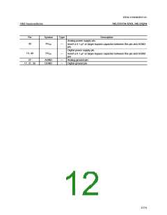
Analog power supply pin.
AVDD
DVDD
Insert a 0.1 µF or larger bypass capacitor between this pin and AGND
pin.
Digital power supply pin.
13, 40
—
Insert a 0.1 µF or larger bypass capacitor between this pin and DGND
pin.
27
AGND
DGND
—
—
Analog ground pin.
Digital ground pin.
17, 31, 39
9/31

 OKI [ OKI ELECTRONIC COMPONETS ]