E S I
E S I
Excel Semiconductor inc.
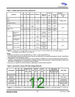
If the system writes the autoselect command
sequence, the device enters the Autoselect mode.
The system can then read some useful codes such
as manufacturer and device ID from the internal reg-
isters on DQ7 - DQ0. Standard read cycle timings
apply in this mode. In the Autoselect mode, the fol-
lowing four informations can be accessed through
either autoselect command method or A9 high-volt-
age autoselect method. Refer to the Table 2.
Flash memory, enabling the system to read the
boot-up firmware from the Flash memory.Refer to
the AC Characteristics tables for RESET# parame-
ters and to Fig. 19 for the timing diagram.
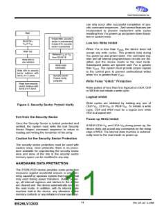
SECTOR GROUP PROTECTION
The ES29LV320 features hardware sector group
protection. A sector group consists of two or more
adjacent sectors that are protected or unprotected
at the same time. In the device, sector protection is
performed on the group of sectors previously
defined in the Table 3-4. Once after a group of sec-
tors are protected, any program or erase operation
is not allowed in the protected sector group. The
previously protected sectors must be unprotected
by one of the unprotect methods provided here
before changing data in those sectors. Sector pro-
tection can be implemented via two methods.
-
-
-
-
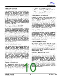
Manufacturer ID
Device ID
Security Sector Lock-indicator
Sector protection verify
Hardware Device Reset ( RESET# )
The RESET# pin provides a hardware method of
resetting the device to read array data. When the
RESET# pin is driven low for at least a period of t
,
RP
the device immediately terminates any operation in
progress, tristates all output pins, and ignores all
read/write commands for the duration of the
RESET# pulse The device also resets the internal
state machine to reading array data. The operation
that was interrupted should be reinitiated once after
the device is ready to accept another command
sequence, to ensure data integrity.
-
-
In-system protection
A9 High-voltage protection
To check whether the sector group protection was
successfully executed or not, another operation
called “protect verification” needs to be per-
formed after the protection operation on a group of
sectors. All protection and protect verifications pro-
vided in the device are summarized in detail at the
Table 1.
CMOS Standby during Device Reset
Current is reduced for the duration of the RESET#
In-System Protection
pulse. When RESET# is held at Vss
device draws the greatly reduced CMOS standby
current ( I ). If RESET# is held at V but not
+ 0.3V, the
“In-system protection”, the primary method,
requires V (11.5V~12.5V) on the RESET# with
CC4
IL
ID
within Vss+0.3V, the standby current will be greater.
A6=0, A1=1, and A0=0. This method can be imple-
mented either in-system or via programming equip-
ment. This method uses standard microprocessor
bus cycle timing. Refer to Fig. 29 for timing diagram
and Fig. 3 for the protection algorithm.
RY/BY# and Terminating Operations
If RESET# is asserted during a program or erase
operation, the RY/BY# pin remains a “0” (busy) until
the internal reset operation is completed, which
A9 High-Voltage Protection
requires a time of t
(during Embedded Algo-
READY
rithms). The system can thus monitor RY/BY# to
determine whether the reset operation is completed.
If RESET# is asserted when a program or erase
operation is not executing (RY/BY# pin is “1”), the
“High-voltage protection”, the alternate method
intended only for programming equipment, must
force V (11.5~12.5V) on address pin A9 and con-
ID
trol pin OE# with A6=0, A1=1 and A0=0. Refer to
Fig. 31 for timing diagram and Fig. 5 for the protec-
tion algorithm.
reset operation is completed within a time of t
READY
(not during Embedded Algorithms). The system can
read data after the RESET# pin returns to V , which
IH
SECTOR UNPROTECTION
requires a time of t
RH.
The previously protected sectors must be unpro-
tected before modifying any data in the sectors.
The sector unprotection algorithm unprotects all
sectors in parallel. All unprotected sectors must first
RESET# tied to the System Reset
The RESET# pin may be tied to the system reset cir-
cuitry. A system reset would thus also reset the
8
Rev. 2D Jan 5, 2006
ES29LV320D

 EXCELSEMI [ EXCEL SEMICONDUCTOR INC. ]