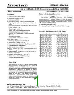
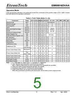
EM68916DVAA
EtronTech
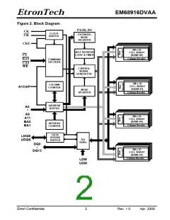
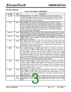
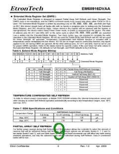
Pin Descriptions
Table 2. Pin Details of EM68916D
Symbol
CK,
Type
Description
Differential Clock: CK and CK are differential clock inputs. All address and
control input signals are sampled on the crossing of the positive edge of CK and
Input
CK
negative edge ofCK . Input and output data is referenced to the crossing of CK
and CK (both directions of the crossing)
CKE
Input
Clock Enable: CKE activates (HIGH) and deactivates (LOW) the CK signal.
Internal clock signals and device input buffers and output drivers. Taking CKE Low
provides Precharge Power Down and Self Refresh operation (all banks idle) or
Active Power Down (Row Active in any bank). CKE is synchronous for all functions
except for disabling outputs, which is asynchronous. Input buffers, excluding
CK,
and CKE, are disabled during Power Down and Self Refresh modes to
CK
reduce standby power consumption.
Bank Activate: BA0 and BA1 define to which bank the BankActivate, Read, Write,
or BankPrecharge command is being applied. BA0 and BA1 also determine which
mode register (MRS or EMRS) is loaded during a Mode Register Set command.
BA0, BA1
A0-A11
Input
Input
Address Inputs: A0-A11 are sampled during the BankActivate command (row
address A0-A11) and Read/Write command (column address A0-A8 with A10
defining Auto Precharge).
Input
Input
Chip Select:
enables (sampled LOW) and disables (sampled HIGH) the
CS
CS
command decoder. All commands are masked when
is sampled HIGH.
CS
provides for external bank selection on systems with multiple banks. It is
CS
considered part of the command code.
Row Address Strobe: The
signal defines the operation commands in
signals and is latched at the positive edges of
RAS
RAS
WE
conjunction with the
and
CAS
CS
CK. When
and
are asserted "LOW" and
is asserted "HIGH," either
CAS
RAS
the BankActivate command or the Precharge command is selected by the
WE
is asserted "HIGH," the BankActivate command is selected
signal. When the
WE
and the bank designated by BA is turned on to the active state. When the
is
WE
asserted "LOW," the Precharge command is selected and the bank designated by
BA is switched to the idle state after the precharge operation.
Input
Input
Column Address Strobe: The
signal defines the operation commands in
CAS
CAS
conjunction with the
and
WE
signals and is latched at the positive edges of
RAS
CK. When
is held "HIGH" and
is asserted "LOW," the column access is
RAS
CS
started by asserting
"LOW." Then, the Read or Write command is selected
CAS
"HIGH " or LOW"."
by asserting
WE
Write Enable: The
signal defines the operation commands in conjunction
signals and is latched at the positive edges of CK. The
WE
WE
and
CAS
with the
RAS
input is used to select the BankActivate or Precharge command and Read or
WE
Write command.
Bidirectional Data Strobe: DQS is an output with read data and an input with
write data. DQS is edge-aligned with read data, centered in write data. It is used to
capture data. For x16, LDQS is DQS for DQ0-DQ7 and UDQS is DQS for DQ8-
DQ15.
LDQS, UDQS
Input /
Output
Etron Confidential
3
Rev. 1.0
Apr. 2009

 ETRON [ ETRON TECHNOLOGY, INC. ]