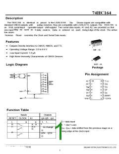
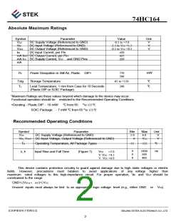
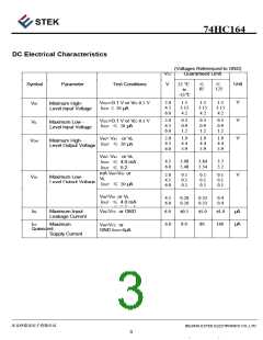
74HC164
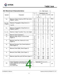
AC Electrical Characteristics
(CL =50pF,Input tr =tf
Guaranteed Limit
V
CC
Symbol
Parameter
V
25 C
to
≤85 C ≤125 C Unit
-55 C
2.0
4.5
6.0
6.0
30
35
4.8
24
28
4.0
20
24
MHz
ns
f
max
Maximum Clock Frequency (50% Duty Cycle)
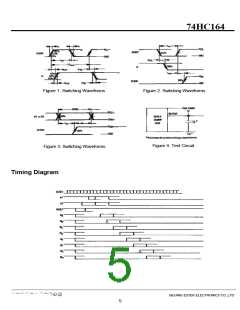
(Figures 1 and 4)
2.0
4.5
6.0
175
35
30
220
44
37
265
53
45
t
PLH, tPHL
(Figures
Maximum Propagation Delay,Clock to Q
1 and 4)
2.0
4.5
6.0
205
41
35
255
51
43
310
62
53
ns
tPHL
Maximum Propagation Delay,Reset to Q
(Figures 2 and 4)
2.0
4.5
6.0
75
15
13
95
19
16
110
22
19
ns
t
TLH, tTHL
Maximum Output Transition Time, Any Output
Maximum Input Capacitance
CIN
-
10
10
10
pF
ns
2.0
4.5
6.0
50
10
9
65
13
11
75
15
13
tSU
Minimum Setup Time,A1 or A2 to Clock
(Figure 3)
2.0
4.5
6.0
5
5
5
5
5
5
5
5
5
ns
ns
ns
ns
ns
t
h
Minimum Hold Time, Clock to A1 or A2
(Figure 3)
2.0
4.5
6.0
5
5
5
5
5
5
5
5
5
trec
Minimum Recovery Time, Reset Inactive to
Clock (Figure 2)
80
16
14
100
20
17
120
24
20
tw
Minimum Pulse Width, Reset (Figure 2)
Minimum Pulse Width, Clock (Figure 1)
Maximum Input Rise and Fall Times (Figure 1)
2.0
4.5
6.0
80
16
14
100
20
17
120
24
20
tw
2.0
4.5
6.0
1000
500
400
1000
500
400
1000
500
400
t
r,
t
f
2.0
4.5
6.0
Power Dissipation Capacitance (Per Package)
Used to determine the no-load dynamic power
consumption:
Typical @25 C,VCC=5.0 V
CPD
140
pF
2f+ICC
V
CC
P =CPDV
D
BEIJING ESTEK ELECTRONICS CO.,LTD
4

 ESTEK [ Estek Electronics Co. Ltd ]