ESMT
M12L64322A
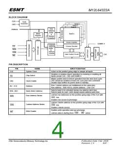
PIN
NAME
INPUT FUNCTION
Makes data output Hi-Z, tSHZ after the clock and masks the output.
Blocks data input when DQM active.
DQM0~3
Data Input / Output Mask
DQ0 ~ DQ31
Data Input / Output
Data inputs / outputs are multiplexed on the same pins.
Power and ground for the input buffers and the core logic.
VDD / VSS
Power Supply / Ground
Isolated power supply and ground for the output buffers to provide
improved noise immunity.
VDDQ / VSSQ
Data Output Power / Ground
No Connection
N.C
This pin is recommended to be left No Connection on the device.
ABSOLUTE MAXIMUM RATINGS
Parameter
Symbol
VIN, VOUT
VDD, VDDQ
TSTG
Value
Unit
V
Voltage on any pin relative to VSS
Voltage on VDD supply relative to VSS
Storage temperature
-1.0 ~ 4.6
-1.0 ~ 4.6
-55 ~ +150
V
°C
W
Power dissipation
PD
IOS
1
Short circuit current
50
mA
Note : Permanent device damage may occur if ABSOLUTE MAXIMUM RATING are exceeded.
Functional operation should be restricted to recommended operating condition.
Exposure to higher than recommended voltage for extended periods of time could affect device reliability.
DC OPERATING CONDITION
Recommended operating conditions (Voltage referenced to VSS = 0V, TA = 0 to 70°C )
Parameter
Supply voltage
Symbol
VDD, VDDQ
VIH
Min
3.0
2.0
-0.3
2.4
-
Typ
3.3
3.0
0
Max
Unit
V
Note
3.6
Input logic high voltage
Input logic low voltage
Output logic high voltage
Output logic low voltage
Input leakage current
VDD+0.3
V
1
VIL
0.8
-
V
2
VOH
-
V
IOH = -2mA
IOL = 2mA
3
VOL
-
0.4
5
V
IIL
-5
-
μ A
Output leakage current
IOL
-5
-
5
μ A
4
Note: 1. VIH(max) = 4.6V AC for pulse width ≤ 10ns acceptable.
2. VIL(min) = -1.5V AC for pulse width ≤ 10ns acceptable.
3. Any input 0V ≤ VIN
VDD + 0.3V, all other pins are not under test = 0V.
4. Dout is disabled , 0V ≤ VOUT ≤ VDD.
≤
Elite Semiconductor Memory Technology Inc.
Publication Date: Feb. 2008
Revision: 2.4 5/47

 ESMT [ ELITE SEMICONDUCTOR MEMORY TECHNOLOGY INC. ]