EN29LV160A
EN29LV160A
16 Megabit (2048K x 8-bit / 1024K x 16-bit) Flash Memory
Boot Sector Flash Memory, CMOS 3.0 Volt-only
FEATURES
• 3.0V, single power supply operation
• JEDEC Standard program and erase
- Minimizes system level power requirements
commands
• High performance
• JEDEC standard DATA# polling and toggle
- Access times as fast as 70 ns
bits feature
• Low power consumption (typical values at 5
• Single Sector and Chip Erase
MHz)
- 9 mA typical active read current
- 20 mA typical program/erase current
- Less than 1 µA standby current
• Sector Unprotect Mode
• Embedded Erase and Program Algorithms
• Erase Suspend / Resume modes:
Read and program another Sector during
Erase Suspend Mode
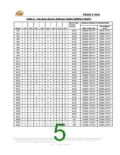
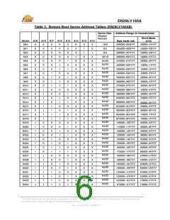
• Flexible Sector Architecture:
- One 16-Kbyte, two 8-Kbyte, one 32-Kbyte,
and thirty-one 64-Kbyte sectors (byte mode)
- One 8-Kword, two 4-Kword, one 16-Kword
and thirty-one 32-Kword sectors (word mode)
• Triple-metal double-poly triple-well CMOS
Flash Technology
• Sector protection :
• Low Vcc write inhibit < 2.5V
- Hardware locking of sectors to prevent
program or erase operations within individual
sectors
• minimum 100K program/erase endurance
cycle
- Additionally, temporary Sector Group
Unprotect allows code changes in previously
locked sectors.
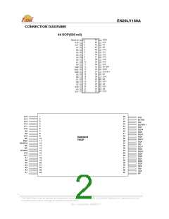
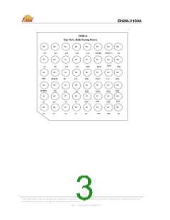
• Package Options
- 44-pin SOP
- 48-pin TSOP (Type 1)
- 48 ball 6mm x 8mm TFBGA
• High performance program/erase speed
- Byte/Word program time: 8µs typical
- Sector erase time: 500ms typical
- Chip erase time: 17.5s typical
• Commercial and Industrial Temperature
Range
GENERAL DESCRIPTION
The EN29LV160A is a 16-Megabit, electrically erasable, read/write non-volatile flash memory,
organized as 2,097,152 bytes or 1,048,576 words. Any byte can be programmed typically in 8µs.
The EN29LV160A features 3.0V voltage read and write operation, with access times as fast as
70ns to eliminate the need for WAIT states in high-performance microprocessor systems.
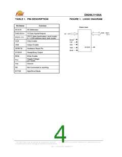
The EN29LV160A has separate Output Enable (OE#), Chip Enable (CE#), and Write Enable
(WE#) controls, which eliminate bus contention issues. This device is designed to allow either
single Sector or full chip erase operation, where each Sector can be individually protected against
program/erase operations or temporarily unprotected to erase or program. The device can sustain
a minimum of 100K program/erase cycles on each Sector.
.
This Data Sheet may be revised by subsequent versions
or modifications due to changes in technical specifications.
©2004 Eon Silicon Solution, Inc., www.essi.com.tw
1
Rev. I, Issue Date: 2008/07/17

 ESMT [ ELITE SEMICONDUCTOR MEMORY TECHNOLOGY INC. ]